
Device mounting substrate and method of repairing defective device

Active Publication Date: 2006-12-12
SONY CORP
View PDF14 Cites 157 Cited by
  • Summary
  • Abstract
  • Description
  • Claims
  • Application Information

AI Technical Summary

Benefits of technology

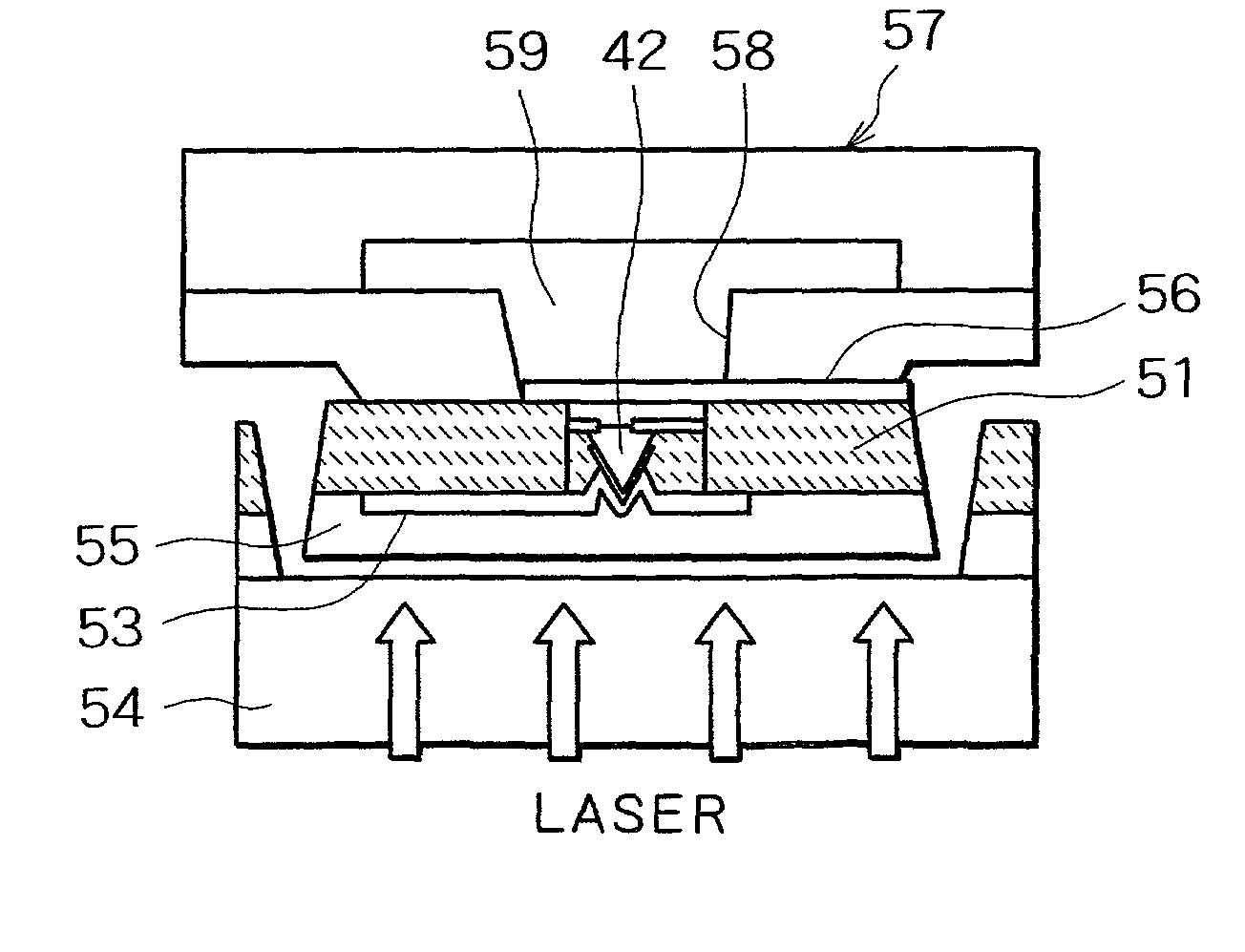
[0007]An object of the present invention is to provide a device mounting substrate and a method of repairing a defective device, which are capable of easily repairing a defective device without any complicated, microscopic work. Another object of the present invention is to provide an image display unit and a method of producing the image display unit, which are capable of quickly repairing, if a non-activated, defective pixel occurs, the defective pixel.
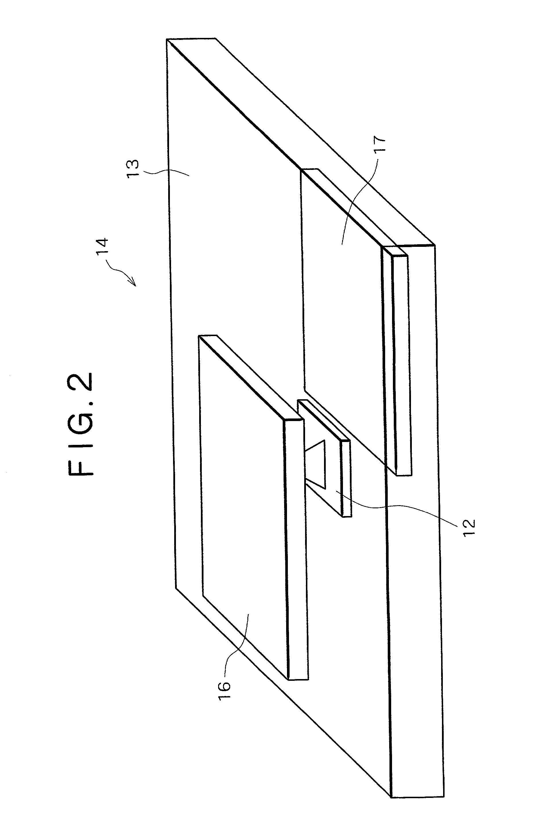
[0010]With the device mounting substrate and the defective device repairing method according to the first and second embodiments of the present invention, a defective device can be repaired by a simple step that is carried out simply mounting and fixing a repair device without removal of the defective device. For example, it is possible to eliminate the need for complicated works such as removal of the mounted devices and selective removal and repair of an insulating layer. Accordingly, a defective device can be repaired not only in the production line but also after shipping of a final product.
[0013]With the image display unit and its production method according to the third and fourth embodiments of the present invention, an image display potion is formed by re-arraying light emitting devices in such a manner that the devices are enlargedly spaced from each other to be arrayed into a matrix. Accordingly, light emitting devices formed in a dense state, that is, with a high degree of integration by fine processing can be effectively re-arrayed in such a manner that the devices are enlargedly spaced from each other to be arrayed into a matrix. As a result, it is possible to significantly improve the productivity of the image display unit. Also, a non-activated pixel due to a defective light emitting device can be easily repaired, without the need for developing a new process.

Problems solved by technology

In the case of thin display units such as LCDs and PDPs, as is apparent from characteristics of the production process thereof, a defective (non-activated) pixel inevitably occurs, and such a defective pixel cannot be repaired.
However, if the defective device is repaired in the usual manner, then the repair requires complicated, microscopic works such as removal of the defective device forcibly fixed, and repair of an insulating layer, and the like.

Method used


Image

  • Device mounting substrate and method of repairing defective device
  • Device mounting substrate and method of repairing defective device
  • Device mounting substrate and method of repairing defective device

Examples


Embodiment Construction

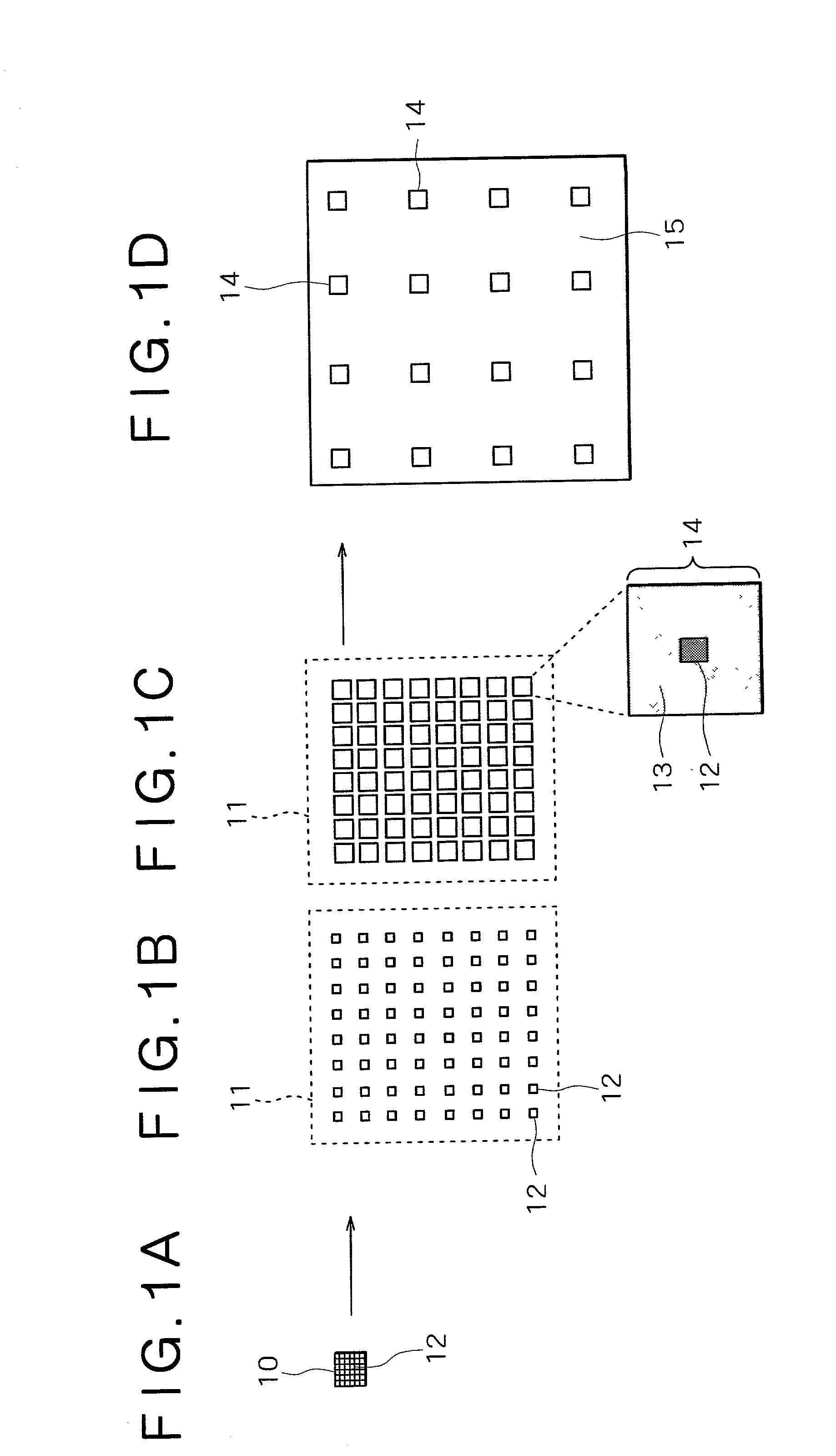
[0054]Hereinafter, a device mounting substrate and a method of repairing a defective device to which the present invention is applied, and an image display unit and a method of producing the image display unit to which the device mounting substrate and the method of repairing a defective device are applied will be described in detail with reference to the drawings. In addition, the following description will be made by example of an image display unit produced by making use of re-array of devices based on a two-step enlarged transfer method.

[0055]First, basic configurations of a method of arraying devices and a method of producing an image display unit, which are based on the two-step enlarged transfer method, will be described. The method of arraying devices and the method of producing an image display unit, which are based on the two-step enlarged transfer method, are carried out by a manner of enlargedly transferring devices formed on a first substrate at a high density onto a te...


PUM


Abstract

A method of repairing a defective one of devices mounted on substrate is provided. Devices are arrayed on a substrate and electrically connected to wiring lines connected to a drive circuit, to be thus mounted on the substrate. The devices mounted on the substrate are then subjected to an emission test. If a defective device is detected in this test, a repair device is mounted at a position corresponding to a position of the defective device. At this time, after wiring lines connected to the defective device are cut off, the repair device is electrically connected to portions of the wiring lines, the portions of the wiring lines being located at positions nearer to the drive circuit side than the cut-off positions of the wiring lines. Since a defective device is repaired by a simple step that is carried out by simply mounting and fixing a repair device without removal of the defective device, it is possible to eliminate the need for any complicated, microscopic work; for example, removal of the mounted devices, and / or selective removal or repair of an insulating layer.

Description

BACKGROUND OF THE INVENTION[0001]The present invention relates to a device mounting substrate in which a defective device has been repaired with a repair device and a method of repairing the defective device, and to an image display unit using the device mounting substrate and a method of producing the image display unit.[0002]The production of an image display unit by arraying light emitting devices in a matrix to build up the devices into the image display unit has been generally performed by two methods. One method, which is used for producing liquid crystal displays (LCDs) or plasma display panels (PDPs), is carried out by directly forming devices on a substrate. The other method, which is used for producing light emitting diode (LED) displays, is carried out by packaging each LED, and arraying the single LED packages on a substrate. For example, in the case of producing image display units such as LCDs or PDPs, since device isolation is impossible from the viewpoint of the stru...

Claims


Application Information

Patent Timeline
IPC IPC(8): H01L21/00H01L27/15H01L31/12G09F9/30G09F9/00G09F9/33G09G3/00H01L21/60H01L33/00H01L33/08H01L33/48
CPCG09G3/006H01L22/22H01L24/24H01L24/25H01L24/82G02F1/1309H01L2221/68368H01L2224/24225H01L2224/24226H01L2224/32225H01L2224/73267H01L2924/01004H01L2924/01012H01L2924/01013H01L2924/01015H01L2924/01039H01L2924/01046H01L2924/01075H01L2924/01078H01L2924/01079H01L2924/01082H01L2924/01005H01L2924/01006H01L2924/01033H01L2924/12041H01L2924/00H01L2924/12042
Inventor OOHATA, TOYOHARUIWAFUCHI, TOSHIAKIOHBA, HISASHI
Owner SONY CORP
Learn More