Wiring substrate, display device, semiconductor chip, and electronic equipment

Inactive Publication Date: 2006-12-12
BOE TECH GRP CO LTD
View PDF10 Cites 12 Cited by
  • Summary
  • Abstract
  • Description
  • Claims
  • Application Information

AI Technical Summary

Benefits of technology

[0013]In the wiring substrate having this arrangement, the guard wiring fabricated of an electrically conductive oxide is arranged between adjacent metal wirings. When a voltage difference occurs between the adjacent metal wirings, corrosion of the metal wiring working as an anode is prevented from dissolving even in the relationship of a cathode and anode setting which occurs in the adjacent metal wirings. In this way, electrical performance of the wiring substrate is maintained at a desired level for a long period of time.
[0036]Since the guard wiring fabricated of the electrically conductive oxide is interposed between adjacent metal wirings in the built-in wiring substrate, the anode metal wiring is prevented from being corroded in the relationship of cathode and anode even when a voltage difference occurs between adjacent metal wirings. In this way, electrical performance of the substrate forming the display device is maintained at a desired level for a long period of time. Also, excellent image quality is maintained for a long period of time.

Problems solved by technology

Routing a long line of ITO trace on the substrate results in a high electrical resistance, making it impossible to normally operate a driving circuit.
On the other hand, the APC or Cr wiring pattern is subject to corrosion and subsequent damage, and presents difficulty in maintaining the quality of wiring.

Method used


Image

  • Wiring substrate, display device, semiconductor chip, and electronic equipment
  • Wiring substrate, display device, semiconductor chip, and electronic equipment
  • Wiring substrate, display device, semiconductor chip, and electronic equipment

Examples


second embodiment

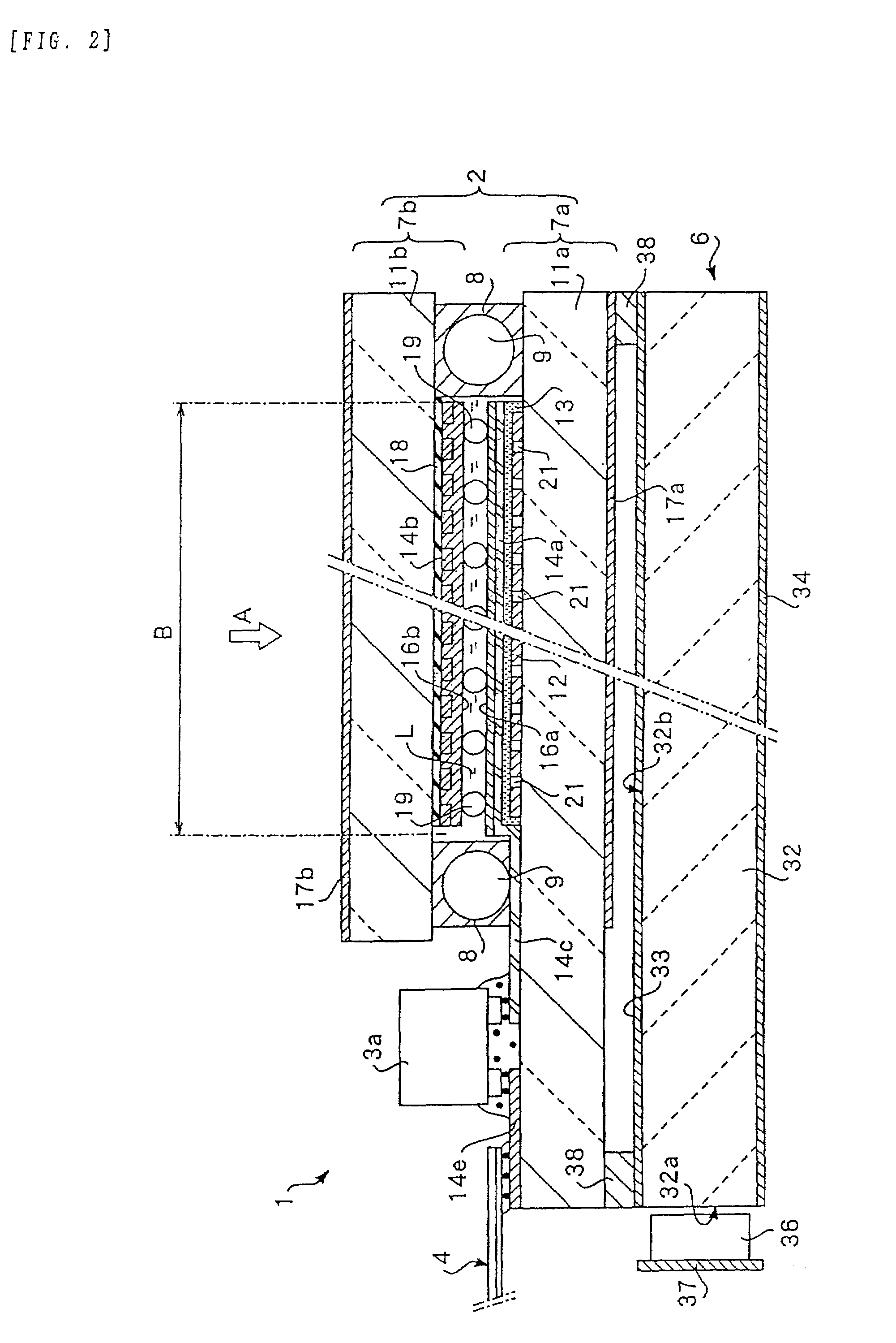
[0090]The second embodiment shown in FIG. 5 is different from the embodiment shown in FIG. 4 in that the ITO is removed from the top of the metal wiring 14e. Even when the ITO is not laminated on the metal wiring 14e, the anode metal wiring is protected from corrosion.

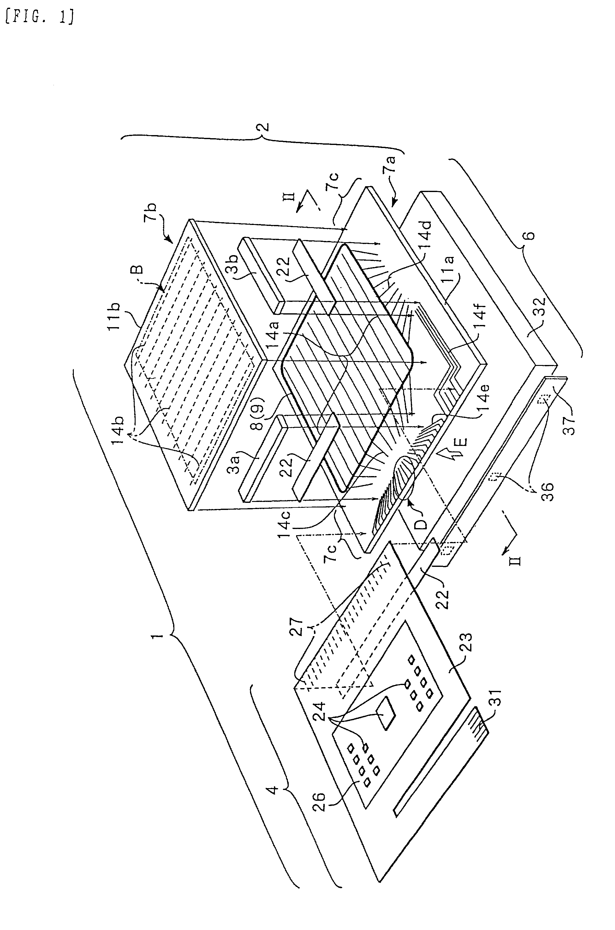
[0091]FIG. 6 shows a third embodiment, which is a modification of the metal wiring shown in FIG. 4. The third embodiment shown in FIG. 6 remains identical to the embodiment shown in FIG. 4 in that voltages V1–V4 of different voltage levels are supplied to a plurality of metal wirings 14e, in that the guard wiring 29 of the electrically conductive oxide ITO is interposed between the anode metal wiring 14e supplied with a high voltage and the cathode metal wiring 14e supplied with a low voltage, and in that the metal wiring 14e is covered with the ITO that forms the guard wiring 29.

third embodiment

[0092]The difference of the third embodiment shown in FIG. 6 from the embodiment shown in FIG. 4 is that the guard wiring 29 is disconnected from an ITO covering layer 41 of the metal wiring 14e. The guard wiring 29 is set to be floating. In this case as well, the anode metal wiring is protected from corrosion.

fourth embodiment

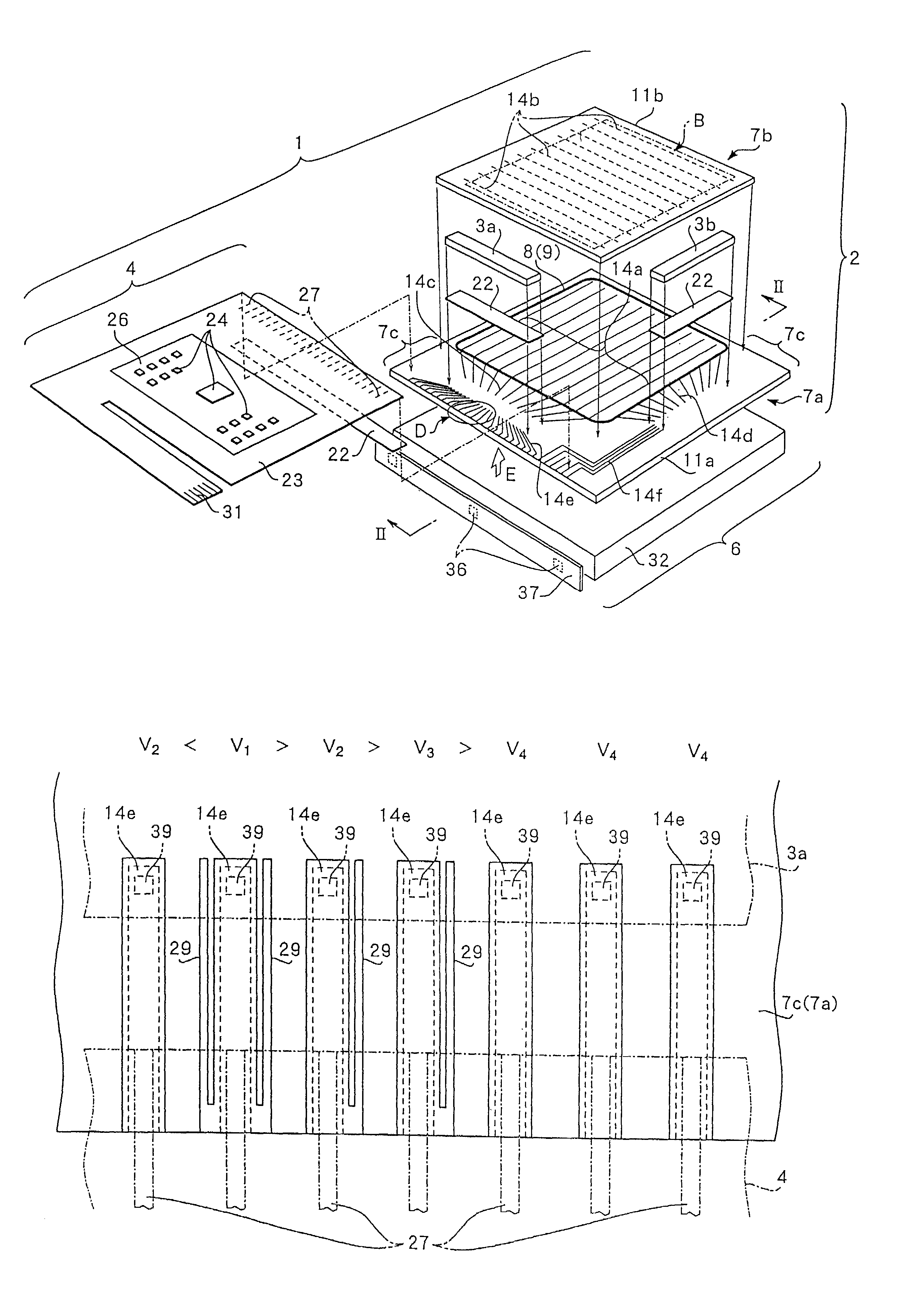
[0093]FIG. 7 and FIG. 8 show the wiring substrate of the present invention. The structure of the wiring substrate shown here is applied to the connection section between the substrate extension area 7c of the first substrate 7a and the metal wiring terminals 27 of the FPC 4.

[0094]In the fourth embodiment, the first substrate 7a shown in FIG. 7(a) functions as one wiring substrate element, and the FPC 4 shown in FIG. 7(b) functions as the other wiring substrate element. These wiring substrate elements are connected to each other as shown in FIG. 8. Specifically, the FPC 4 is connected to the substrate extension area 7c of the first substrate 7a using the ACF 22 as shown in FIG. 1, and a single substrate is thus constructed of the first substrate 7a and the FPC 4 as a unit.

[0095]Referring to FIG. 7(a), in this embodiment, the metal wiring 14e is fabricated of a metal such as an APC alloy on the surface of the substrate extension area 7c, and a covering layer 41 fabricated of an electr...


PUM


Abstract

A wiring substrate is formed of a plurality of metal wirings 14e formed on a substrate 7c. A guard wiring 29 fabricated of an electrically conductive oxide such as ITO is interposed between at least a pair of adjacent ones of a plurality of metal wirings 14e. When voltages V1, V2, V3, and V4 applied to the metal wirings 14e are related to be V1>V2>V3>V4, a guard wiring 29 is present between a metal wiring 14e functioning as an anode and a metal wiring 14e functioning as a cathode, and the anode metal wiring 14e is prevented from being corroded.

Description

BACKGROUND OF THE INVENTION[0001]1. Technical Field of the Invention[0002]The present invention relates to a wiring substrate having a metal wiring formed on a substrate, a display device including the wiring substrate, a semiconductor chip for use in the wiring substrate, and electronic equipment employing one of the display device and the wiring substrate.[0003]2. Description of the Related Art[0004]A display device such as a liquid-crystal device is widely used as a display in electronic equipment such as a mobile computer, a mobile telephone, a video camera, etc. An EL (Electro-luminescence) device is beginning to be used as one of display units. The liquid-crystal device includes a pair of electrodes, and an electrooptical material interposed between the electrodes. By controlling a voltage applied between the electrodes, the orientation of the liquid crystal is controlled. When the orientation of the liquid crystal is controlled, light transmitted through the liquid crystal is...

Claims


Application Information

Patent Timeline
IPC IPC(8): H05K1/16G02F1/1345H05K3/22G09F9/00G09F9/30H01L23/12H01L27/32H05K1/02H05K1/03H05K1/09
CPCG02F1/1345H05K1/0256H05K1/0306H05K2201/0326H05K2201/0761H05K2201/0769H05K2201/09781H01L2224/16225H01L2224/32225H01L2224/73204H01L2224/05573H01L2224/05568H01L2224/04026H01L2924/00014H01L2924/00H01L2224/05599H05K3/22
Inventor ARUGA, YASUHITOYATABE, SATOSHIENDO, KOGOHARADA, NORIHITO
Owner BOE TECH GRP CO LTD
Why Eureka
Try Eureka