IC chip package structure and underfill process

a chip and packaging technology, applied in the direction of electrical equipment, semiconductor devices, semiconductor/solid-state device details, etc., can solve the problems of affecting the chip, requiring a large number of solder bumps, and crowding of solder bumps along the perimeter of the flip chip, so as to reduce stress, prevent or reduce stress

Active Publication Date: 2006-12-12
TAIWAN SEMICON MFG CO LTD
View PDF6 Cites 41 Cited by
  • Summary
  • Abstract
  • Description
  • Claims
  • Application Information

AI Technical Summary

Benefits of technology

[0013]In accordance with these and other objects and advantages, the present invention is generally directed to a novel underfill process for reducing stress applied to corners of a flip chip in an IC package structure during the application of an adhesive material between the flip chip and a carrier substrate. The process includes providing a dam structure on a carrier substrate; attaching solder bumps of an inverted flip chip to the carrier substrate; injecting an adhesive material between the flip chip and the carrier substrate at multiple injection points located along adjacent edges of the flip chip; and injecting a sealant material around the adhesive material. During application of the adhesive material and the sealant material to the IC package structure in the underfill process, the dam structure reduces stress applied to the corners of the flip chip. This prevents or at least reduces de-lamination of dielectric layers on the flip chip.
[0014]The present invention further includes an integrated circuit chip structure having a carrier substrate; multiple dam elements provided on the carrier substrate; and a flip chip attached to the carrier substrate, with respective corners of the flip chip disposed adjacent to the respective dam elements. During assembly of the IC chip structure, an adhesive material is injected at multiple injection points at respective edges of the flip chip to reduce stress at the corners of the flip chip. A sealant material is provided around the adhesive material.

Problems solved by technology

Consequently, ambient air is able to penetrate the package and adversely affect the chip over time.
Because of the numerous functions typically performed by the microcircuitry of a flip chip, a relatively large number of solder bumps are often required.
The size of a flip chip is typically on the order of about thirteen millimeters per side, resulting in crowding of the solder bumps along the perimeter of the flip chip.

Method used


Image

  • IC chip package structure and underfill process
  • IC chip package structure and underfill process
  • IC chip package structure and underfill process

Examples


Embodiment Construction

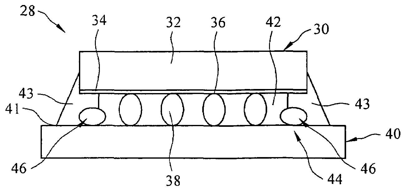
[0021]The present invention generally contemplates a novel underfill process for reducing stress applied to corners of a flip chip in assembly of an IC package structure, particularly during the application of an adhesive material between the flip chip and a carrier substrate. According to the process, a dam structure is provided on a carrier substrate. The dam structure typically includes multiple dam elements provided adjacent to respective corners of the carrier substrate. A flip chip having multiple solder bumps is then inverted, and the solder bumps on the flip chip are bonded to the carrier substrate. A high-stress modulus adhesive material, which is typically an epoxy resin, is injected between the flip chip and the carrier substrate at multiple injection points located along respective edges of the flip chip. Finally, a low-stress modulus sealant material, which is typically an epoxy resin containing rosin, is injected around the adhesive material. As the adhesive material a...


PUM


Abstract

A novel integrated circuit (IC) chip package structure and underfill process which reduces stress applied to corners of a flip chip in an IC package structure during the application of an adhesive material between the flip chip and a carrier substrate is disclosed. The process includes providing a dam structure on a carrier substrate; attaching solder bumps of an inverted flip chip to the carrier substrate; injecting an adhesive material between the flip chip and the carrier substrate at multiple injection points located along adjacent edges of the flip chip; and injecting a sealant material around the adhesive material. During application of the adhesive material and the sealant material to the IC package structure in the underfill process, the dam structure reduces stress applied to the corners of the flip chip. This prevents or at least reduces de-lamination of dielectric layers on the flip chip.

Description

FIELD OF THE INVENTION[0001]The present invention relates to flip chip packaging of integrated circuit (IC) semiconductor assemblies. More particularly, the present invention relates to a novel IC chip package structure and underfill process for an IC chip package structure which utilizes dams in conjunction with directional injection of an underfill bonding material between a chip and a substrate to prevent or reduce de-lamination of intermetal dielectric (IMD) layers on a ball grid array (BGA) flip chip during IC chip package assembly.BACKGROUND OF THE INVENTION[0002]One of the last processes in the production of semiconductor integrated circuits (IC) is multi-leveled packaging, which includes expanding the electrode pitch of the IC chips containing the circuits for subsequent levels of packaging; protecting the chip from mechanical and environmental stress; providing proper thermal paths for channeling heat dissipated by the chip; and forming electronic interconnections. The mann...

Claims


Application Information

Patent Timeline
Patent Type & Authority Patents(United States)
IPC IPC(8): H01L23/495H01L23/48
CPCH01L21/563H01L24/29H01L2224/16225H01L2224/26175H01L2924/01019H01L2924/01006H01L2224/32225H01L2924/3025H01L2924/14H01L2924/01082H01L2924/01075H01L2924/0105H01L2224/73203H01L2224/73204H01L2224/83102H01L2224/92125H01L2924/01015H01L2924/01033H01L2924/00H01L2924/3512H01L2224/0554H01L2224/05567H01L2224/05573H01L2924/00014H01L2224/05599H01L2224/0555H01L2224/0556
Inventor LEE, HSIN-HUILEE, CHIEN-HSIUN
Owner TAIWAN SEMICON MFG CO LTD
Why Eureka
Try Eureka