Plasma display panel

a plasma display and surface discharge technology, applied in the direction of gas discharge electrodes, gas discharge vessels/containers, gas-filled discharge tubes, etc., can solve the problems of deterioration in the brightness of the displayed picture, and achieve the effect of improving the fineness of the picture and reducing the brightness of the display

Inactive Publication Date: 2006-12-12
PANASONIC CORP
View PDF21 Cites 1 Cited by
  • Summary
  • Abstract
  • Description
  • Claims
  • Application Information

AI Technical Summary

Benefits of technology

[0017]It is a first object of the present invention to provide an improved plasma display panel capable of ensuring an improved fineness for a picture being displayed on the panel, without causing the above-mentioned problems such as a decrease in a displaying brightness and some misdischarges in discharge cells.
[0018]It is a second object of the present invention to provide an improved plasma display panel capable of preventing a reflection of an external light incident on the panel, thereby improving the contrast of a picture being displayed on the panel.
[0019]It is a third object of the present invention to provide an improved plasma display panel capable having an improved resolution.
[0020]It is a fourth object of the present invention to provide an improved plasma display panel capable of preventing a warpage in partition walls (which are provided to divide a discharge space into a plurality of discharge cells), thereby preventing a possible deformation in the predetermined shape of the discharge cells.
[0021]It is a fifth object of the present invention to provide an improved plasma display panel capable of preventing the formation of unwanted slots between a front glass substrate and a rear glass substrate, thereby avoiding any possible defect caused by such slots in the display panel.

Problems solved by technology

However, with the above-described surface discharge type AC-driven plasma display panel, if it is desired to improve the fineness of a displayed picture by reducing the size of each discharge cell C′, a total surface area of the fluorescent layer 6 will also be undesirably reduced, resulting in a deterioration in the brightness of the displayed picture.
This, however, would cause a problem called discharge interference between every two adjacent discharge cells C′, hence resulting in some misdischarges.

Method used


Image

  • Plasma display panel
  • Plasma display panel
  • Plasma display panel

Examples


first embodiment

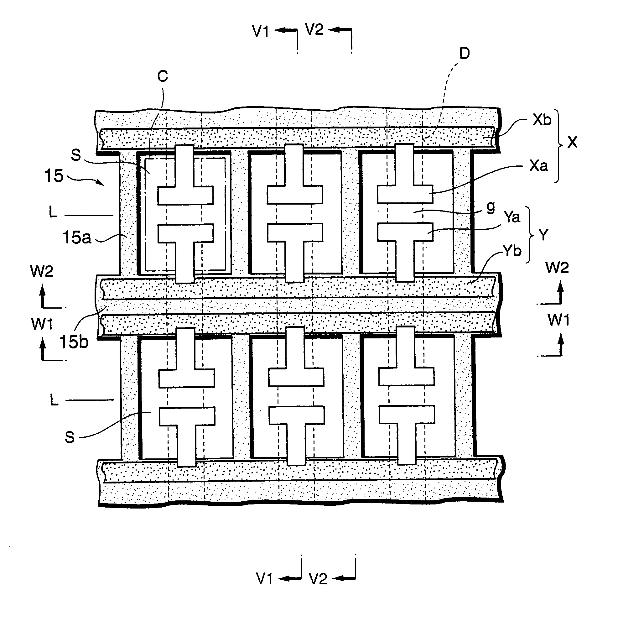
[0101]A first embodiment of the present invention is illustrated in FIGS. 1–5.

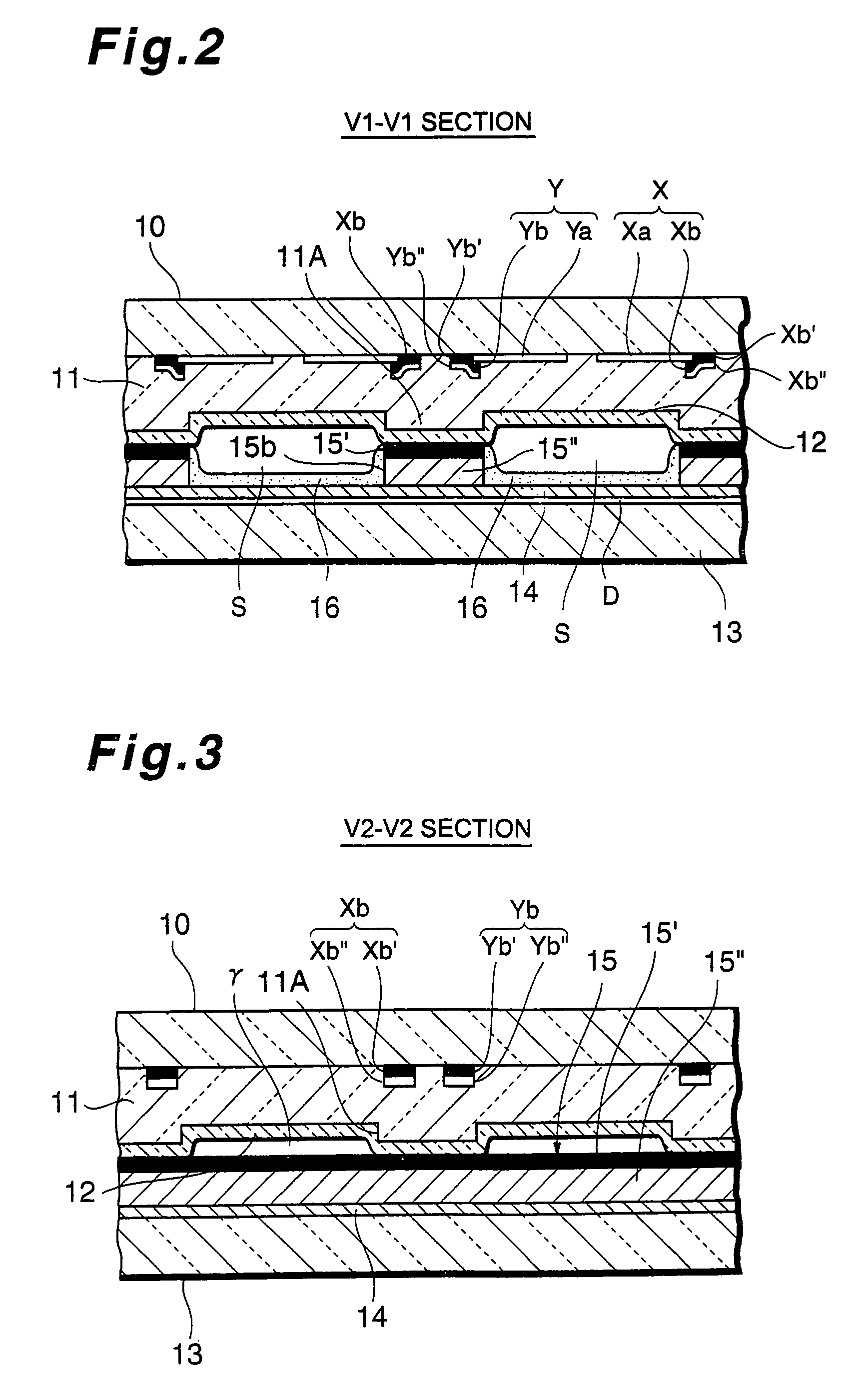
[0102]Referring to FIGS. 1–5, a surface discharge type AC-driven plasma display panel of the present invention has a front glass substrate 10 serving as a displaying surface for the panel, a plurality of row electrode pairs (X,Y) mutually parallelly disposed on the inner surface of the front glass substrate 10.

[0103]Each row electrode X includes a plurality of T-shaped transparent electrodes Xa consisting of a transparent electrically conductive film made of ITO, and an elongated bus electrode Xb consisting of a metal film which is connected with one end of each T-shaped transparent electrode Xa.

[0104]Similarly, each row electrode Y includes a plurality of T-shaped transparent electrodes Ya consisting of a transparent electrically conductive film made of ITO, and an elongated bus electrode Yb consisting of a metal film which is connected with one end of each T-shaped transparent electrode Ya.

[0105]Further,...

second embodiment

[0139]A second embodiment of the present invention is illustrated in FIG. 6.

[0140]As shown in FIG. 6, a plasma display panel according to the second embodiment includes a plurality of displaying lines Li, Li+1 . . . , along which there are disposed row electrodes (Xi, Yi) in accordance with an arrangement of (Yi, Xi), (Xi+1, Yi+1) . . . in the column direction of the panel.

[0141]In this way, T-shaped transparent electrodes (Xai, Xai+1) of mutually adjacent row electrodes (Xi, Xi+1) are allowed to be connected to a common (elongated) bus electrode Xbj, thus enabling a total area occupied by the elongated bus electrodes to be smaller than that in the plasma display panel of the first embodiment (FIGS. 1–5).

[0142]Further, each lateral wall 25b of a #-like partition wall assembly 25 is allowed to be narrower in its width than that in the plasma display panel of the first embodiment (FIGS. 1–5), thus ensuring each discharge space S1 to be larger than that in the first embodiment, thereby...

third embodiment

[0145]A third embodiment of the present invention is illustrated in FIG. 7.

[0146]As shown in FIG. 7, a plasma display panel according to the third embodiment includes a plurality of displaying lines Li−1′, Li′, Li+1′ . . . , along which there are disposed row electrodes (Xi′, Yi′), in accordance with an arrangement of (Yi−1′, Xi−1′), (Xi′, Yi′), (Yi+1′, Xi+1′) . . . in the column direction of the panel.

[0147]In fact, T-shaped transparent electrodes (Xai−1′, Xai′) of mutually adjacent row electrodes (Xi−1′, Xi′) are allowed to be connected to a common (elongated) bus electrode Xbj′, transparent electrodes (Yai′, Yai+1′) of mutually adjacent row electrodes (Yi′, Yi+1′) are allowed to be connected to a common (elongated) bus electrode Ybj′.

[0148]In this way, with respect to mutually adjacent displaying lines (Li−1′, Li′), mutually adjacent row electrodes (Xi−1′,Xi′) are allowed to use a common bus electrode Xbj′. Similarly, with respect to mutually adjacent displaying lines (Li′, Li+1′...


PUM


Abstract

A plasma display panel comprises a front substrate and a rear substrate, a plurality of row electrode pairs provided on the inner surface of the front substrate, a dielectric layer provided on the inner surface of the front substrate for coverring the row electrode pairs, a plurality of column electrodes provided on the inner surface of the rear substrate, a partition wall assembly provided between the front substrate and the rear substrate, said partition wall assembly including a plurality of longitudinal partition walls and a plurality of lateral partition walls, forming a plurality of discharge cells. In particular, the dielectric layer has a plurality of projection portions located corresponding to and protruding toward the lateral partition walls of the partition wall assembly, in a manner such that there would be no slots formed between the dielectric layer and the lateral partition walls.

Description

CROSS-REFERENCE TO RELATED APPLICATION[0001]This is a Divisional Application which claims the benefit of pending U.S. patent application Ser. No. 10 / 083,290, filed Feb. 27, 2002, which is a Divisional Application of U.S. patent application Ser. No. 09 / 466,841, filed Dec. 20, 1999 (now U.S. Pat. No. 6,465,956, issued on Oct. 15, 2002). The disclosures of the prior applications are hereby incorporated herein in their entirety by reference.BACKGROUND OF THE INVENTION[0002]The present invention relates to a surface discharge type AC-driven plasma display panel, particularly to the discharge cell structure of such plasma display panel.[0003]Recently, there has been appeared in the market a new type of display device which is large in size and small in thickness, with one example being a surface discharge type AC-driven plasma display panel.[0004]FIG. 47 is a plane view schematically indicating a surface discharge type AC-driven plasma display panel made according to a prior art. FIG. 48 ...

Claims


Application Information

Patent Timeline
Patent Type & Authority Patents(United States)
IPC IPC(8): H01J17/49H01J17/04H01J17/16
CPCH01J11/12H01J11/24H01J11/32H01J11/36H01J11/38H01J2211/245H01J2211/265H01J2211/323H01J2211/326H01J2211/444
Inventor KOSHIO, CHIHARUAMEMIYA, KIMIOKOMAKI, TOSHIHIROTANIGUCHI, HITOSHISAKAI, TATSUROMASUDA, KOSUKE
Owner PANASONIC CORP
Why Eureka
Try Eureka