Multi chip package type memory system and a replacement method of replacing a defect therein

a memory system and multi-chip package technology, applied in static storage, digital storage, instruments, etc., can solve the problems of no effective method, the multi-chip package type memory system itself cannot be used, and the productivity rate of the multi-chip package type memory system is much lower than that of the single memory chip

Inactive Publication Date: 2006-12-12
KK TOSHIBA
View PDF30 Cites 52 Cited by
  • Summary
  • Abstract
  • Description
  • Claims
  • Application Information

AI Technical Summary

Problems solved by technology

Therefore, when the only one of the plurality of the memory chips is defect, even if the others are not defects, the Multi Chip Package (MCP) type memory system itself can not be used.
Therefore, productivity rate of the Multi Chip Package (MCP) type memory system is determined by multiplications of productivity rates of all memory chips in the single package, thereby inevitably resulting in much lower productivity rate of the Multi Chip Package (MCP) type memory system than that of the single memory chip.
Conventionally, in order to make the productivity of the Multi Chip Package (MCP) type memory system higher, there is no effective method other than making productivity of all of the each memory chips higher.
And also, it was very difficult to make the productivity of all memory chips each of which has different function greater.
However, it is practically difficult to use the technique stated in the Japanese patent laid open kokai 2003-59288 due to a high costs and an unstable operation of the MCP type memory system.

Method used


Image

  • Multi chip package type memory system and a replacement method of replacing a defect therein
  • Multi chip package type memory system and a replacement method of replacing a defect therein
  • Multi chip package type memory system and a replacement method of replacing a defect therein

Examples


first embodiment

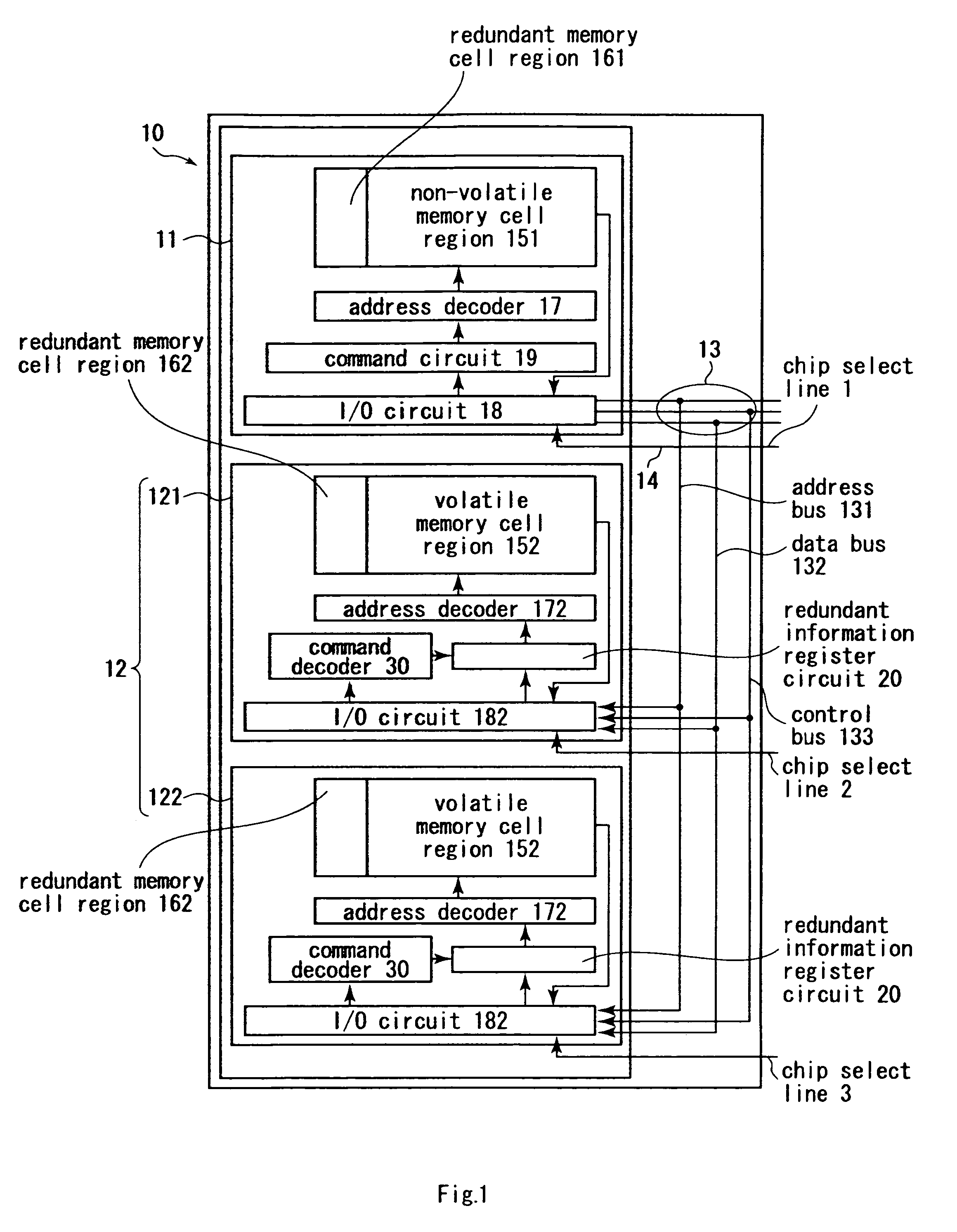
[0034]FIG. 1 shows a schematic block diagram of a multi chip package type memory system of a first embodiment in the present invention. The multi chip package type memory system 10 is used as a part of a memory system.

[0035]The multi chip package type memory system 10 is commonly connected to a system bus to which a CPU (Central Processing Unit), other memory system, and so on are connected. The multi chip package type memory system 10 of the first embodiment in the present invention includes plural kinds of memory chips that include a non-volatile memory chip 11 and volatile memory chips 121 and 122. It should be noted that each of the volatile memory chips 121 and 122 is a different chip each other and the non-volatile memory chip 11.

[0036]Hereinafter, for simplicity to explain, it is assumed that the multi chip package type memory system includes one non-volatile memory chip and two volatile memory chips, but it is not limited to it. For example, the multi chip package type memor...

second embodiment

[0055]In the first embodiment of the present invention, the redundant information that is based on whether a volatile memory cell region 152 has the defect or not is read out from the non-volatile memory chip 12 after applying a power voltage to the multi chip package type memory system. And then, one of the volatile memory chips 121 and 122 which includes the volatile memory cell region 152 is selected. After replacing all the defects to be replaced, an instruction (instructions 7 and 8 shown in FIG. 3) to indicate an end of transmission are issued.

[0056]In case where it is not needed to replace a defect in the volatile memory chip by using the redundant information stored in the non volatile memory chip, a control pad that is fixed at a predetermined voltage is provided in the non volatile memory chip in order to make the transmission of the redundant information invalid. The control pad is connected to a power supply voltage VDD or a ground voltage GND by bonding wire, thereby ma...

third embodiment

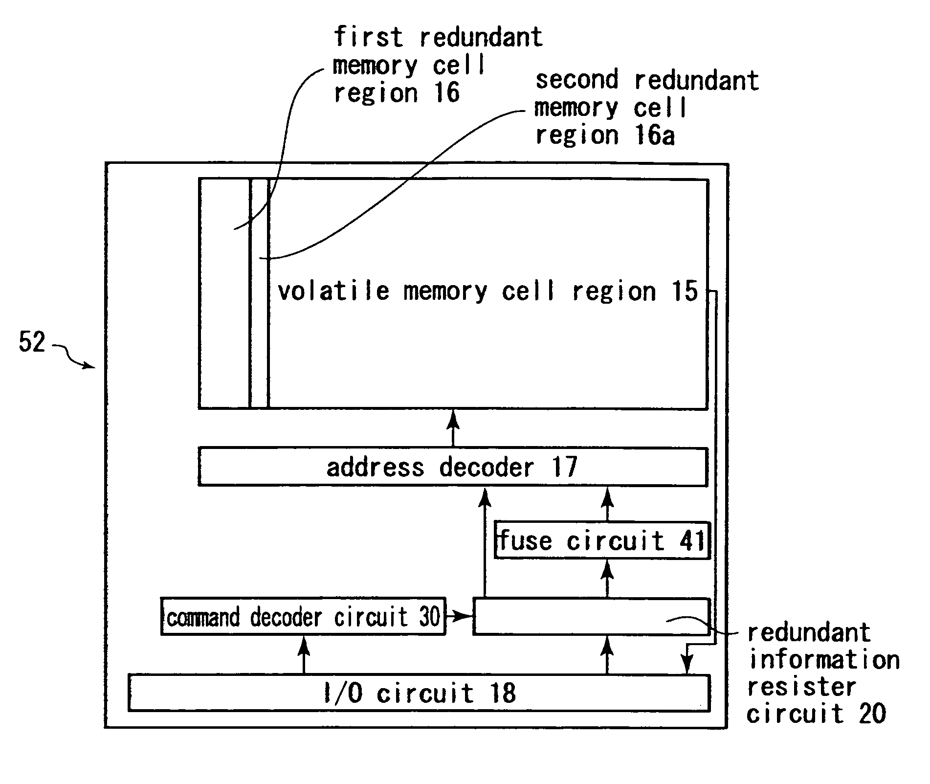
[0057]In the second embodiment of the present invention, the control pad is provided in the non volatile memory chip and connected to a power supply voltage VDD or a ground supply voltage GND by bonding wire in order to make the transmission invalid. On the other hand, the control pad in a third embodiment of the present invention is provided in the volatile memory chip and connected to a power supply voltage VDD or a ground voltage GND by bonding wire, thereby making the transmission invalid. The control pad may be a dedicated pad, or be commonly used as the other pad. And also, instead of providing the control pad, a blow fuse which is provided in the volatile memory chip may be provided in order to make the transmission invalid. For example, when a predetermined blow fuse is cut, the transmission is made invalid.


PUM


Abstract

A multi chip package type memory system comprising a volatile memory chip including a volatile memory cell region configured to store a data and a redundant memory cell region configured to be used to replace a defect in the volatile memory cell region; a non-volatile memory chip including a non-volatile memory cell region, the non-volatile memory chip configured to output a first redundant information that is an information based on whether the volatile memory cell region in the volatile memory chip has the defect or not; and internal line connected between the volatile memory chip and the non-volatile memory chip, the internal line configured to transmit the first redundant information from the non-volatile memory chip to the volatile memory chip, and the internal line configured to transmit at least one of a data, an address signal, and a control signal from / to an outside circuit.

Description

CROSS-REFERENCE TO RELATED APPLICATION[0001]This application is based upon and claims the benefit of priority from the prior Japanese Patent Application No.2003-371007, filed Oct. 30, 2003, the entire contents of which are incorporated herein by reference.BACKGROUND OF THE INVENTION[0002]1. Field of the Invention[0003]This present invention relates to a Multi Chip Package (MCP) type memory system and a replacement method of a replacing a defect therein. For example, the present invention can be used in a computer system, a memory card system, or a mobile phone system that is required to downsize.[0004]2. Description of the Related Art[0005]A recent computer system can be connected to a memory system that comprises of plural kinds of memory integrated circuits that are used as an external memory. When the memory system is used in the computer system (for instance, a mobile terminal), the memory system is strongly required to downsize. And also, recently the Multi Chip Package (MCP) t...

Claims


Application Information

Patent Timeline
Patent Type & Authority Patents(United States)
IPC IPC(8): G11C7/00G06F12/16G11C11/34G11C29/00G11C29/04
CPCG11C29/802G11C5/04G11C29/789
Inventor OKUNO, TAKANOBU
Owner KK TOSHIBA
Why Eureka
Try Eureka