Optoelectronic devices and methods of production

Inactive Publication Date: 2006-12-19
II VI DELAWARE INC
View PDF43 Cites 2 Cited by
  • Summary
  • Abstract
  • Description
  • Claims
  • Application Information

AI Technical Summary

Benefits of technology

[0013]The invention provides production methods and the resulting optoelectronic devices. The optoelectronic devices produced from the method of the invention are particularly well suited for use in device arrays. Devices that can be produced by the method of the invention include, for example, VCSELs, p-n junction (PIN) detectors, and other optoelectronic devices. The preferred devices are VCSELs and are preferably part of an array, an SPA. The devices of the invention are advantageous for inclusion in arrays of the devices because they decrease the parasitic capacitance that limit the effectiveness of the arrays. Parasitic capacitance is decreased by the use of an isolation moat as described herein.

Problems solved by technology

Otherwise, the capacitance reduces switching speed and increases the bit error rate due to noise integrated on the photodetector.
This configuration may be the largest contributor to parasitic capacitance, due to the proximity of the signal line to the common substrate.
However, the size of the anode pad cannot be reduced without compromising yield of the flip-chip interconnect process.
Although this reduces the parasitic capacitance, it does not eliminate it or reduce it to an acceptable level.
VCSELs driven by their anodes are undesirable because it requires use of slower P-channel transistors.
Devices with both sources and detectors can often suffer from “cross-talk”.
This creates an undesirable situation where, for example, the source can alter the detected response and thereby change the perceived signal.

Method used


Image

  • Optoelectronic devices and methods of production
  • Optoelectronic devices and methods of production
  • Optoelectronic devices and methods of production

Examples


Embodiment Construction

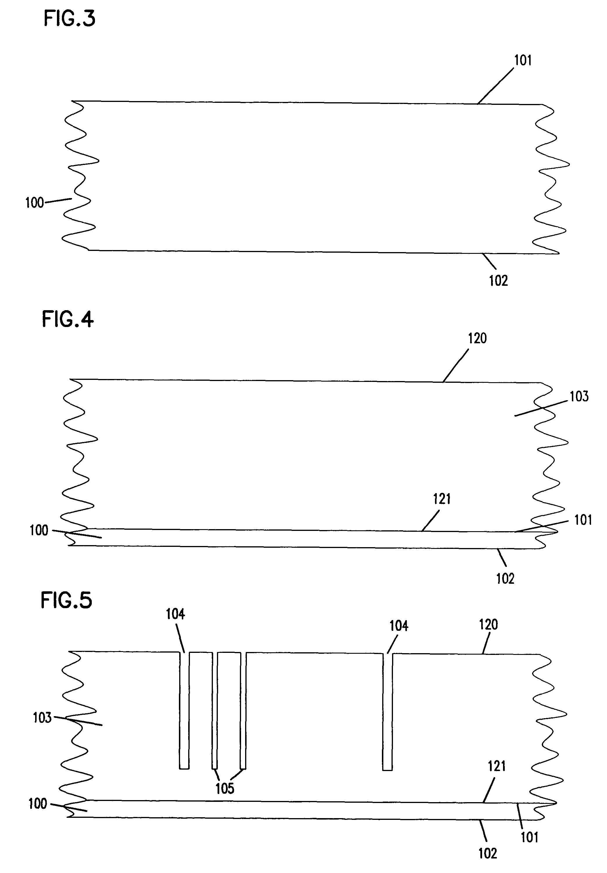
[0020]The invention includes devices and methods of producing the same with at least an optoelectronic structure, isolation moat, and through wafer via. The method of the invention includes producing an optoelectronic structure, forming a through wafer via and forming an isolation moat.

The Device

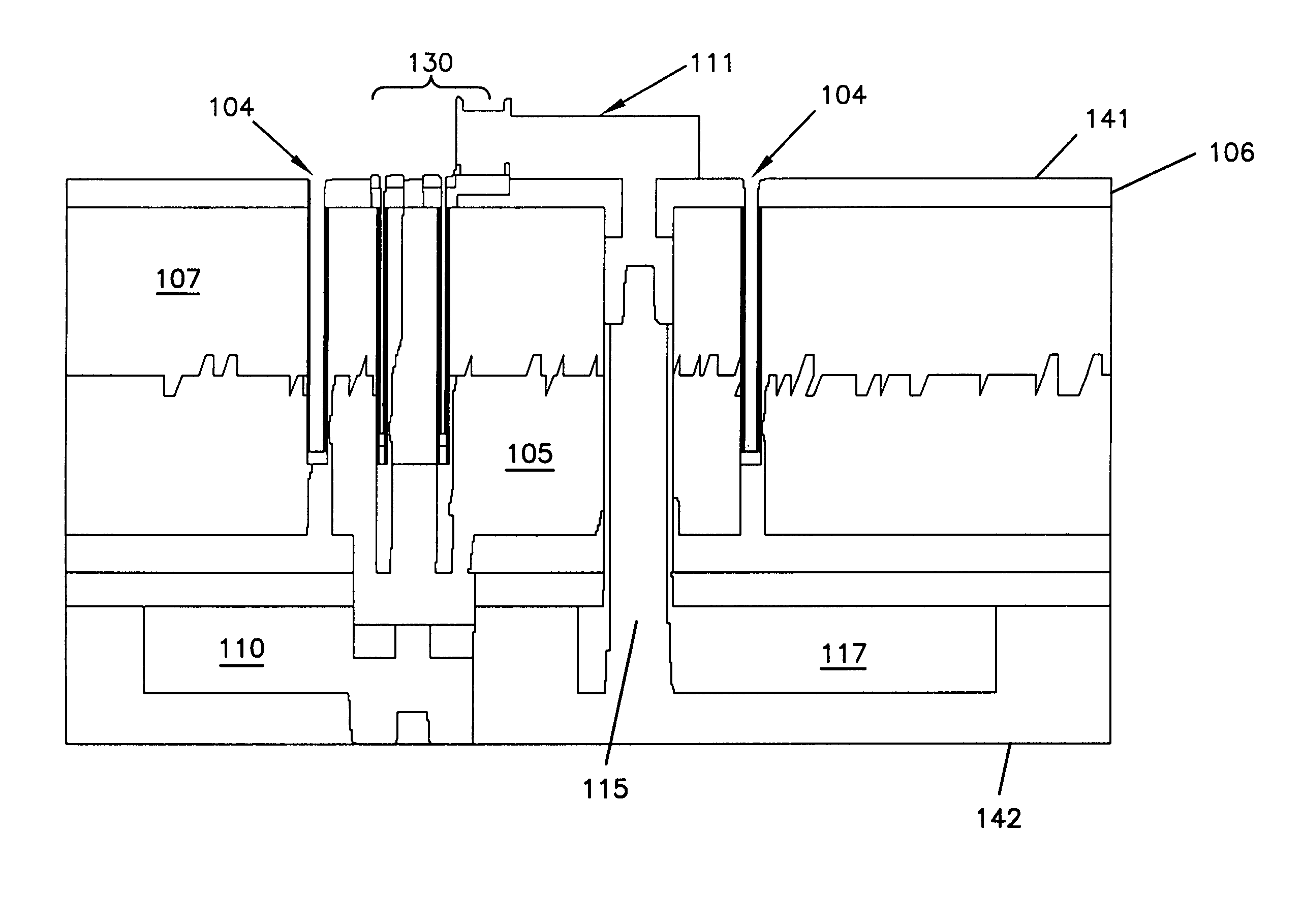
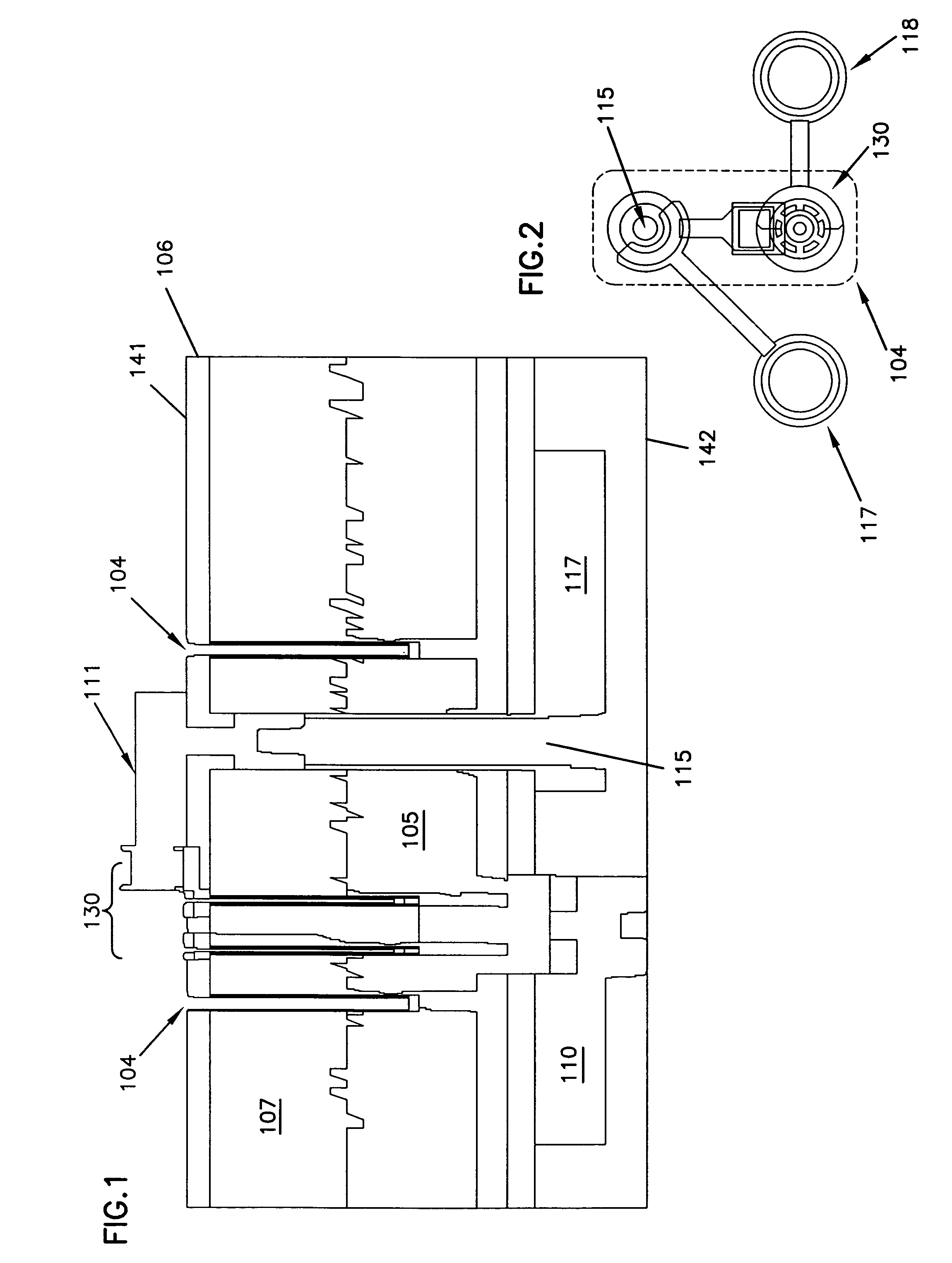
[0021]FIGS. 1 and 2 are sectional views, and it should therefore be appreciated that the illustrations depicted in FIGS. 1 and 2 can extend into and out of the drawings, thereby allowing for the depiction of arrays of the various structures.

[0022]FIG. 1 illustrates a device in accordance with one aspect of the invention. FIG. 1 is a cross sectional view of such an exemplary device. FIG. 2 also illustrates a device in accordance with one aspect of the invention. FIG. 2 is a top view of such an exemplary device showing the spatial layout of the structures given therein. As seen in FIGS. 1 and 2, a device in accordance with the invention comprises an optoelectronic structure 130, an isolation m...


PUM


Abstract

The invention includes both devices and methods of production. A device in accordance with the invention includes a top surface and a bottom surface, a through wafer via extending from the top surface to the bottom surface, an optoelectronic structure and an ion implanted isolation moat, wherein the optoelectronic structure and the through wafer via are enclosed within the isolation moat. A method in accordance with the invention is a method of producing a device that includes the steps of forming an optoelectronic structure, forming a through wafer via, extending from a top surface to a bottom surface of the device and forming an ion implanted isolation moat, wherein the through wafer via and the optoelectronic structure are enclosed by the isolation moat.

Description

[0001]This application is a divisional of application Ser. No. 10 / 037,013, filed Dec. 31, 2001, now U.S. Pat. No. 6,724,798 which application(s) are incorporated herein by reference.UNITED STATES GOVERNMENT RIGHTS[0002]This invention was made with the United States Government support under 70NAHB8H4023 awarded by National Institute of Standards and Technology (NIST).FIELD OF THE INVENTION[0003]The invention generally pertains to a novel production method and the resulting optoelectronic devices. More particularly, the invention pertains to a novel method of producing optoelectronic devices, such as vertical cavity surface emitting lasers (VCSELs) and providing isolated contacts for these devices, enabling their use in high speed, low cost multi-device arrays.BACKGROUND OF THE INVENTION[0004]Smart pixel arrays (SPAs) are devices containing arrays of vertical cavity surface emitting lasers (VCSELs) and photodetectors. SPAs are capable of performing high-speed switching and routing of ...

Claims


Application Information

Patent Timeline
IPC IPC(8): H01S5/00H01L21/768H01L31/12H01S5/042H01S5/183
CPCH01L21/76898H01L31/125H01S5/18311H01S5/0425H01S5/18308H01S5/2063H01S2301/176H01S5/04256H01S5/02345
Inventor LIU, YUEJOHNSON, KLEIN L.BAIER, STEVEN M.
Owner II VI DELAWARE INC
Why Eureka
Try Eureka