Electronic device, surface emitting laser, surface emitting laser array, light source, optical module

Active Publication Date: 2013-08-22
FURUKAWA ELECTRIC CO LTD
View PDF3 Cites 6 Cited by
  • Summary
  • Abstract
  • Description
  • Claims
  • Application Information

AI Technical Summary

Benefits of technology

The present invention offers electronic devices, surfaces emitting lasers, light sources, and optical modules with reduced parasitic capacitance.

Problems solved by technology

However, beyond the case of a surface emitting laser, in a case of an electronic device that operates by application of a modulated electrical signal, problems may occur such as a decrease in the cutoff frequency of the electronic device due to the parasitic capacitance and an increase in crosstalk between components which occurs when the electronic device is configured in an array.

Method used


Image

  • Electronic device, surface emitting laser, surface emitting laser array, light source, optical module
  • Electronic device, surface emitting laser, surface emitting laser array, light source, optical module
  • Electronic device, surface emitting laser, surface emitting laser array, light source, optical module

Examples


first embodiment

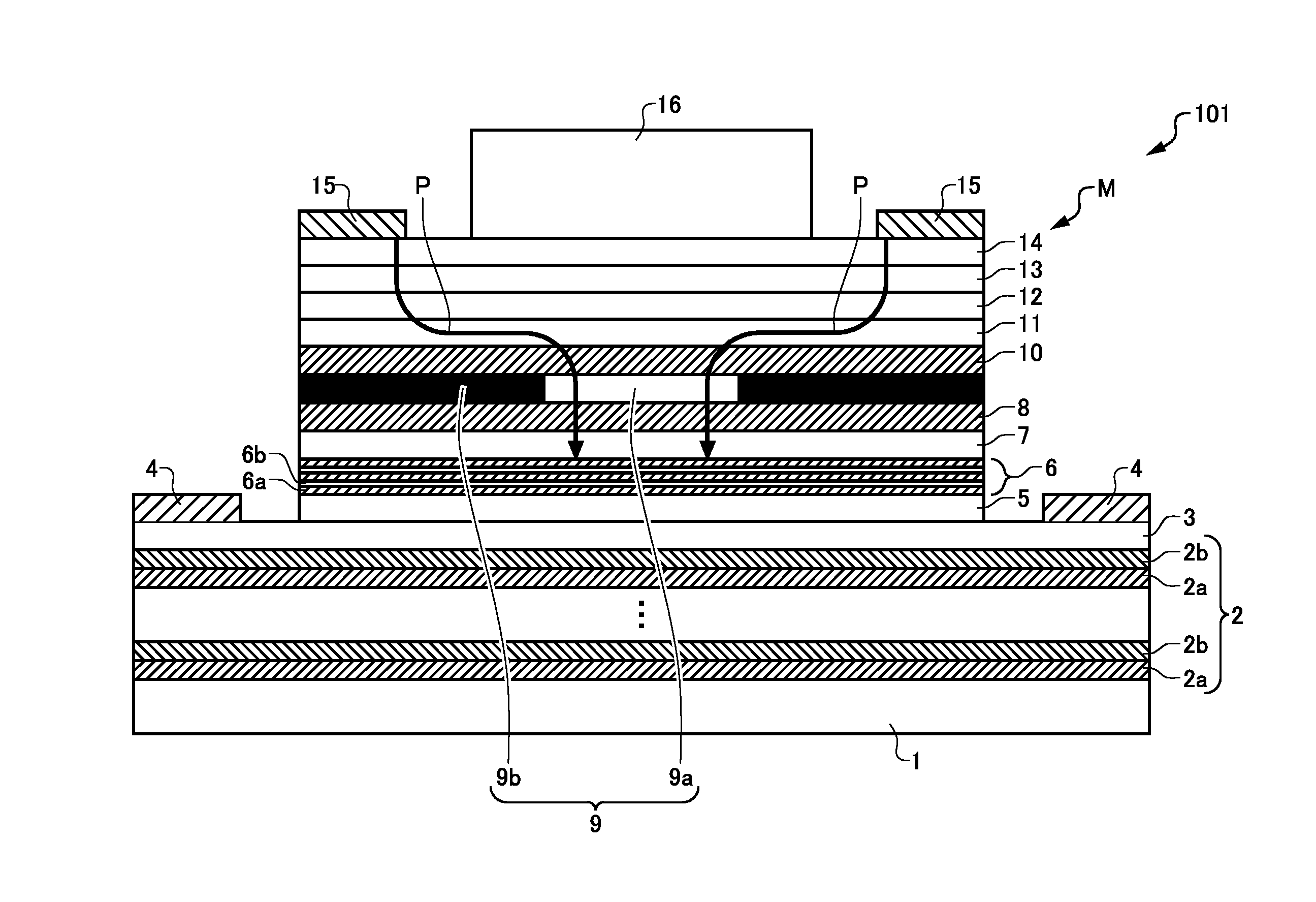
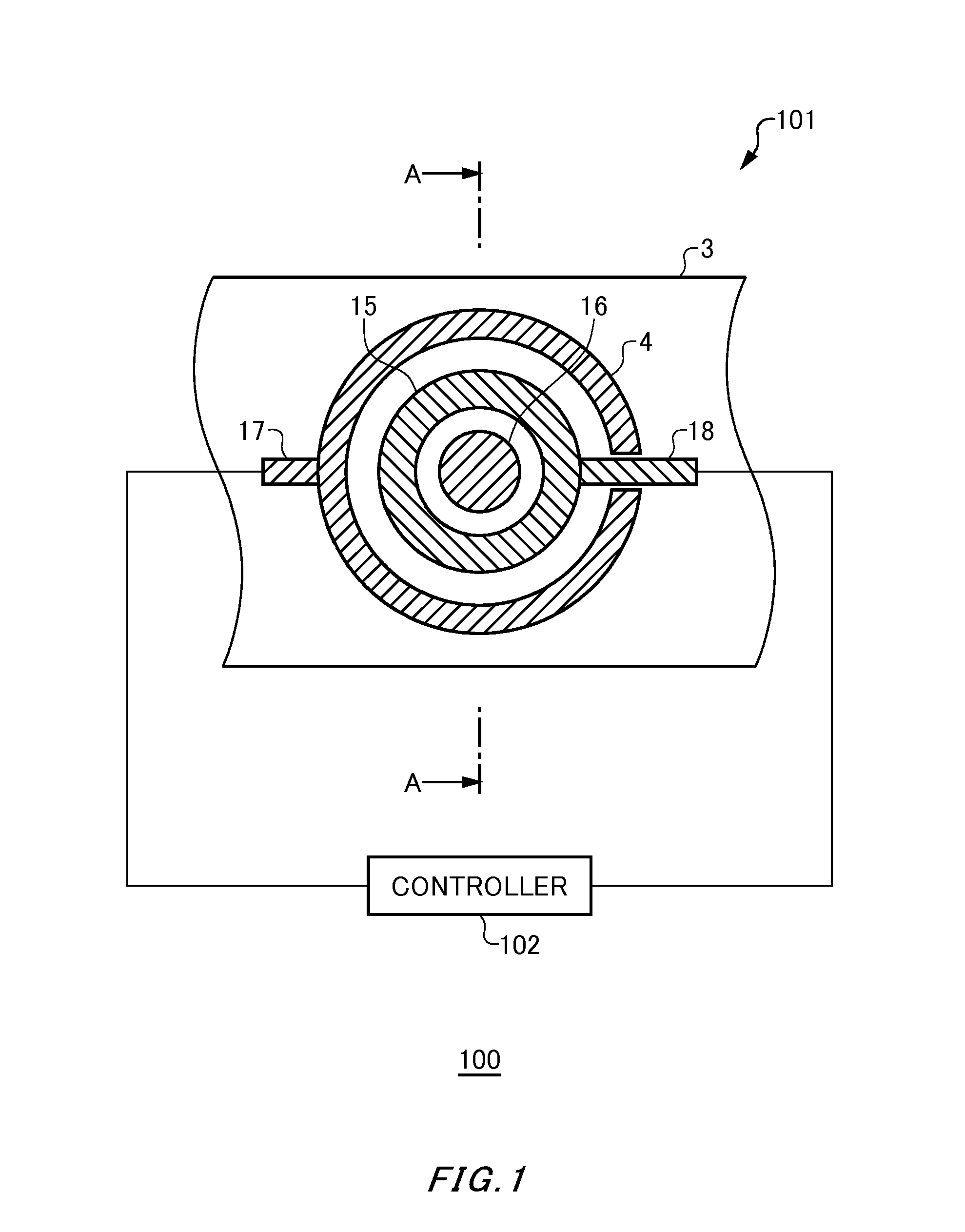
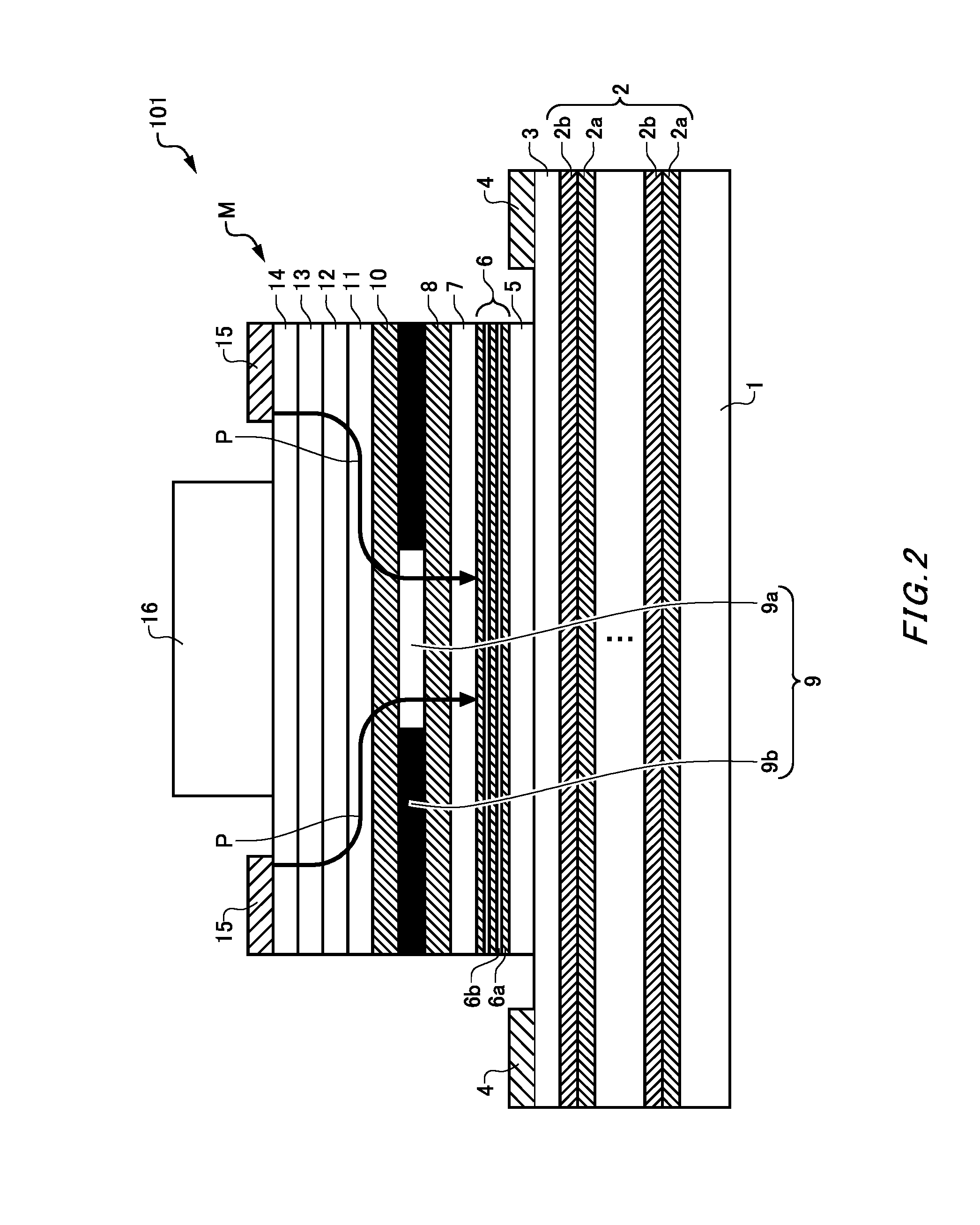
[0048]FIG. 1 is a schematic view of a configuration of a light source 100 according to a first embodiment of the present invention. As shown in FIG. 1, the light source 100 includes a surface emitting laser 101, which is an example of an electronic device, and a controller 102 that controls the surface emitting laser 101. FIG. 2 is a cross-sectional view of the surface emitting laser 101 shown in FIG. 1 over the line A-A.

[0049]As shown in FIGS. 1 and 2, the surface emitting laser 101 includes a lower DBR mirror 2 that functions as a lower multilayer reflective semiconductor mirror, an n-type contact layer 3 that is a lower contact layer, an n-side electrode 4 that is a lower electrode, an n-type cladding layer 5, an active layer 6, a p-type cladding layer 7, a lower graded-composition layer 8, a current confinement layer 9, an upper graded-composition layer 10, a p-type spacer layer 11, a p-type high conductivity layer 12, a p-type spacer layer 13, a p-type contact layer 14 that is ...

second embodiment

[0091]The following describes a second embodiment of the present invention, which is a surface emitting laser array apparatus that uses the surface emitting laser of the present invention and is used in a signal light source, for example, for optical interconnection. FIG. 7 is a schematic perspective view of the surface emitting laser array apparatus according to the second embodiment. As shown in FIG. 7, the surface emitting laser array apparatus 200 is realized by mounting a surface emitting laser array chip 210 on a flat package 201, which is a widely known ceramic leaded chip carrier (CLCC). The surface emitting laser array chip 210 is connected to a metal caster (electrode) 202 by wiring, not shown.

[0092]FIG. 8 is a schematic planar view of the surface emitting laser array chip 210 shown in FIG. 7. As shown in FIG. 8, the surface emitting laser array chip 210 includes a surface emitting laser array section 205 formed by a two-dimensional arrangement of 40 of the surface emittin...

third embodiment

[0096]The following describes a third embodiment of the present invention, which is a surface emitting laser package that is a light source including the surface emitting laser of the present invention and that is used in a signal light source for optical interconnection, for example. FIG. 9 is a schematic cross-sectional view of the surface emitting laser package according to the third embodiment. As shown in FIG. 9, the surface emitting laser package 300 includes a surface emitting laser module 310, a housing 320 that houses the surface emitting laser module 310, a lens 323 that is held above the surface emitting laser module 310 by the housing 320 via an arm 324, an optical fiber mount 321 provided above the housing 320, and an optical fiber 322 that is inserted into and held by the optical fiber mount 321. The surface emitting laser module 310 includes the surface emitting laser 312 of the present invention, a substrate 311 on which the surface emitting laser 312 is mounted, ele...


PUM


Abstract

An electronic device comprising a multilayer semiconductor structure formed by a periodic structure having a first semiconductor layer and a second semiconductor layer, wherein in at least a portion of the multilayer semiconductor structure, the first semiconductor layer and the second semiconductor layer have different conduction types. The first semiconductor layer and the second semiconductor layer have different refractive indexes, and the multilayer semiconductor structure functions as a multilayer reflective mirror. As a result, an electronic device, a surface emitting laser, a surface emitting laser array, a light source, and an optical module with decreased parasitic capacitance can be realized.

Description

[0001]The contents of the following Japanese patent application and PCT application are incorporated herein by reference:[0002]NO. JP2010-225075 filed on Oct. 4, 2010, and[0003]NO. PCT / JP2011 / 005506 filed on Sep. 29, 2011.BACKGROUND[0004]1. Technical Field[0005]The present invention relates to an electronic device, a surface emitting laser (i.e. a vertical cavity surface emitting laser (VCSEL)), a surface emitting laser array, a light source, and an optical module.[0006]2. Related Art[0007]A surface emitting laser having an intra-cavity structure is known as a light source for optical interconnection, as shown in Patent Documents 1 and 2, for example. The intra-cavity structure is a structure in which current is injected into the active layer from inside two reflective mirrors, e.g. DBR (Distributed Bragg Reflector) minors, forming an optical cavity, without passing through the reflective minors in one or both directions.[0008]In the surface emitting laser described in Patent Docume...

Claims


Application Information

Patent Timeline
IPC IPC(8): H01S5/183G02B5/08
CPCH01S5/02284H01S5/02288H01S5/0425H01S5/06226H01S5/18308H01S5/18358H01S5/18369H01S2304/04G02B5/0816H01S5/18311H01L2924/181H01L2224/48091H01L2224/48137H01S5/04257H01S5/02253H01S5/02251H01L2924/00012H01L2924/00014
Inventor SHIMIZU, HITOSHIKAWAKITA, YASUMASA
Owner FURUKAWA ELECTRIC CO LTD
Why Eureka
Try Eureka