Process for forming a patterned thin film structure for in-mold decoration

Inactive Publication Date: 2007-01-02
SIPIX CHEM
View PDF86 Cites 45 Cited by
  • Summary
  • Abstract
  • Description
  • Claims
  • Application Information

AI Technical Summary

Problems solved by technology

The typical photolithographic process comprises several time consuming and high cost steps including (1) forming an unpatterned metal thin film layer (2) coating the metal thin film with photoresist; (3) patterning the photoresist by image-wise exposing it through a photomask to, for example, ultraviolet light; (4) “developing” the patterned image by removing the photoresist from either the exposed or the unexposed areas, depending on the type of photoresist used, to uncover the metal thin film in areas from which it is to be removed (i.e., areas where no thin film material is to be located); (5) using a chemical etching process to remove the thin film from the areas from whic

Method used


Image

  • Process for forming a patterned thin film structure for in-mold decoration
  • Process for forming a patterned thin film structure for in-mold decoration
  • Process for forming a patterned thin film structure for in-mold decoration

Examples


Embodiment Construction

[0017]A detailed description of a preferred embodiment of the invention is provided below. While the invention is described in conjunction with that preferred embodiment, it should be understood that the invention is not limited to any one embodiment. On the contrary, the scope of the invention is limited only by the appended claims and the invention encompasses numerous alternatives, modifications and equivalents. For the purpose of example, numerous specific details are set forth in the following description in order to provide a thorough understanding of the present invention. The present invention may be practiced according to the claims without some or all of these specific details. For the purpose of clarity, technical material that is known in the technical fields related to the invention has not been described in detail so that the present invention is not unnecessarily obscured.

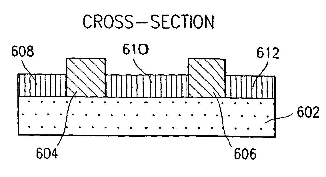
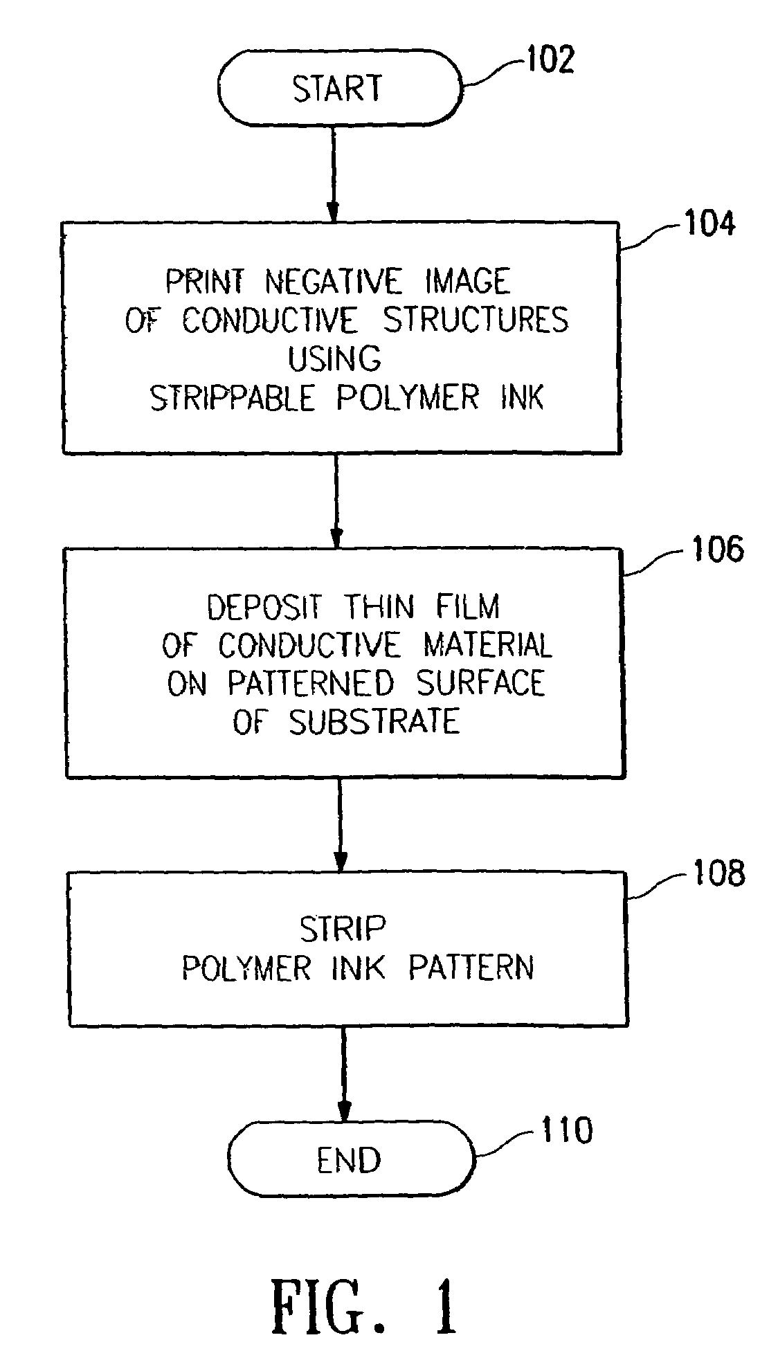
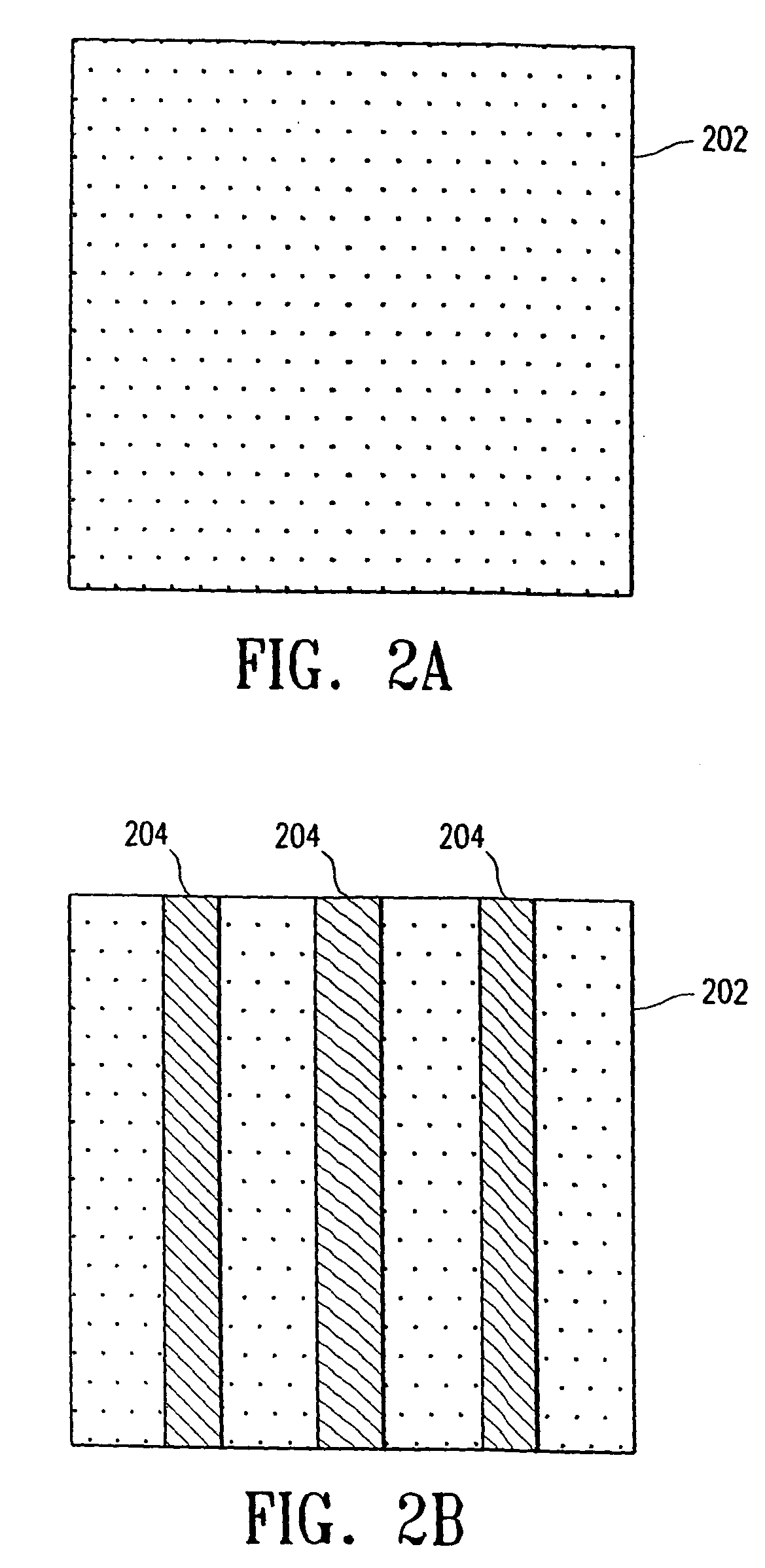
[0018]A process for forming a patterned thin film structure on a substrate is disclosed. In one e...


PUM


Abstract

A process for forming a patterned thin film structure on a substrate or in-mold decoration film is disclosed. A pattern is printed with a material, such as a masking coating or ink, on the substrate, the pattern being such that, in one embodiment, the desired structures will be formed in the areas where the printed material is not present, i.e., a negative image of thin film structure to be formed is printed. In another embodiment, the pattern is printed with a material that is difficult to strip from the substrate, and the desired thin film structures will be formed in the areas where the printed material is present, i.e., a positive image of the thin film structure is printed. The thin film material is deposited on the patterned substrate, and the undesired area is stripped, leaving behind the patterned thin film structure.

Description

CROSS-REFERENCE TO RELATED APPLICATION[0001]This application is a continuation-in-part of co-pending U.S. application Ser. No. 10 / 422,557, filed Apr. 23, 2003, the content of which is incorporated herein by reference in its entirety. Said application Ser. No. 10 / 422,557 claims the benefit of U.S. Provisional Application Ser. No. 60 / 375,902, filed Apr. 24, 2002, the content of which is incorporated herein by reference in its entirety.FIELD OF THE INVENTION[0002]The present invention relates generally to in-mold decoration. A process for forming a patterned thin film on a substrate for in-mold decoration is disclosed.BACKGROUND OF THE INVENTION[0003]In-mold decoration (IMD) has emerged as an increasingly popular set of techniques for decorating injection-molded parts. IMD techniques are used to incorporate text, numbers, legends, other symbols and information, and purely decoratively designs into injection molded parts such as telephones and other consumer electronics, automobile dash...

Claims


Application Information

Patent Timeline
IPC IPC(8): B05D1/32B05D3/10B05D5/12B32B43/00H01L21/31H01L21/36B05C11/11B29CB41M1/30C23C14/04C23C14/08C23C14/20G02F1/1343H01L51/00H05K3/04H05K3/14H05K3/16H05K3/18H05K3/38
CPCB32B38/10C23C14/042C23C14/086C23C14/20G02F1/13439G09F7/165H05K3/04H05K3/048H05K3/386B29C45/14811Y10T156/1189H01L51/0022H05K3/146H05K3/16H05K3/184H05K2201/0317H05K2203/0257H05K2203/0264H05K2203/0522H05K2203/0746Y10S156/922Y10T156/11B29K2995/002H10K71/611
Inventor CHAUG, YI-SHUNGWANG, XIAOJIAKILUK, SEANTSENG, SCOTTZANG, HONGMEILIANG, RONG-CHANG
Owner SIPIX CHEM
Why Eureka
Try Eureka