Plasma processing method and apparatus

a processing method and apparatus technology, applied in the field of plasma processing methods and apparatuses, can solve the problems of complex process and wide range of objects, and achieve the effect of high precision

Inactive Publication Date: 2007-01-02
PANASONIC CORP
View PDF4 Cites 0 Cited by
  • Summary
  • Abstract
  • Description
  • Claims
  • Application Information

AI Technical Summary

Benefits of technology

[0007]In view of the aforementioned conventional issues, an object of the present invention is to provide a plasma processing method and apparatus capable of processing desired fine linear portions with high precision.

Problems solved by technology

However, there is a defect that the process is complicated.
However, the etching by the plasma processing method and apparatus described in connection with the prior art example has had an issue that the object would be processed over a wide range beyond desired fine linear portions.

Method used


Image

  • Plasma processing method and apparatus
  • Plasma processing method and apparatus
  • Plasma processing method and apparatus

Examples


first embodiment

[0079]the present invention is described below with reference to FIGS. 1 to 5.

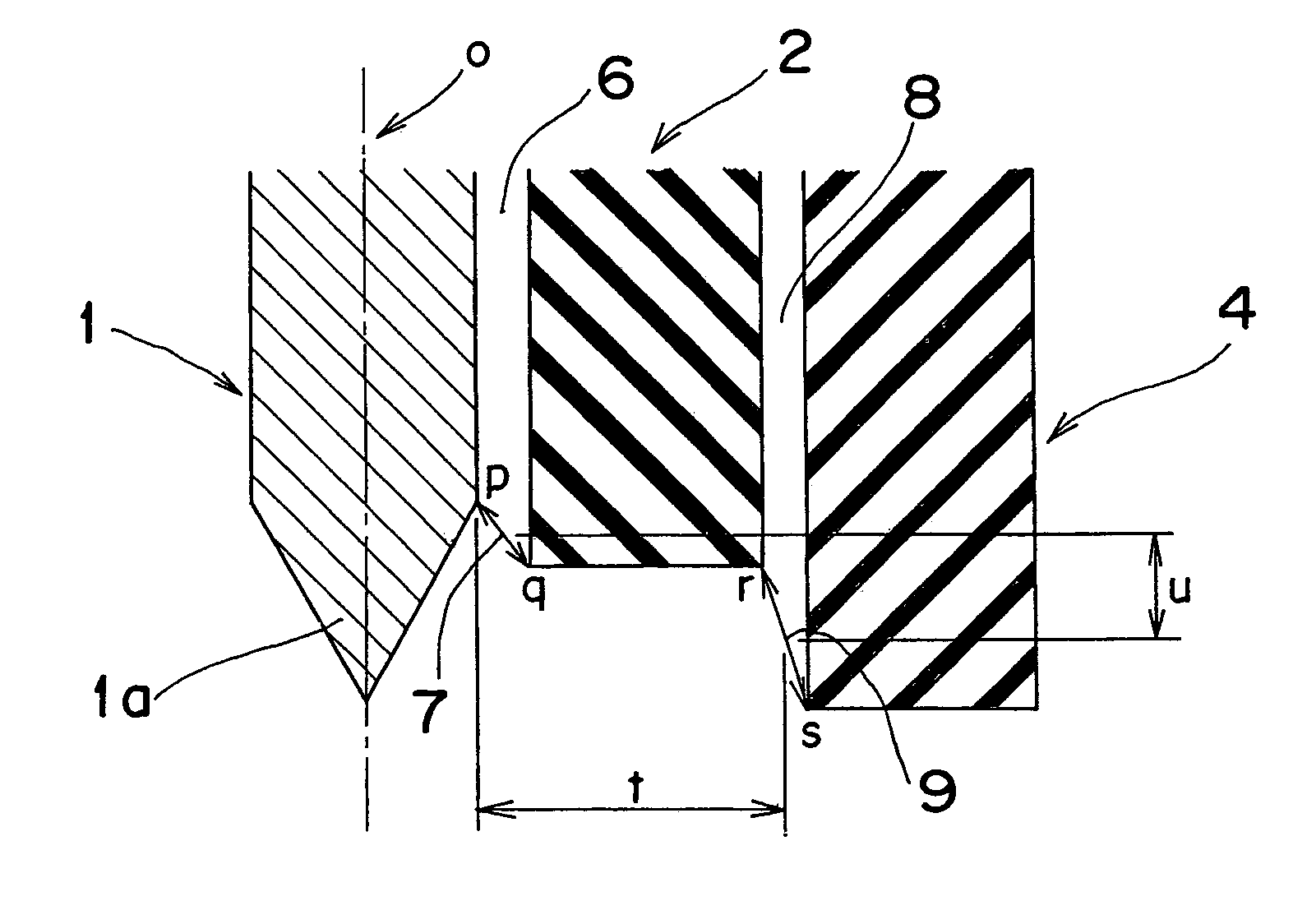
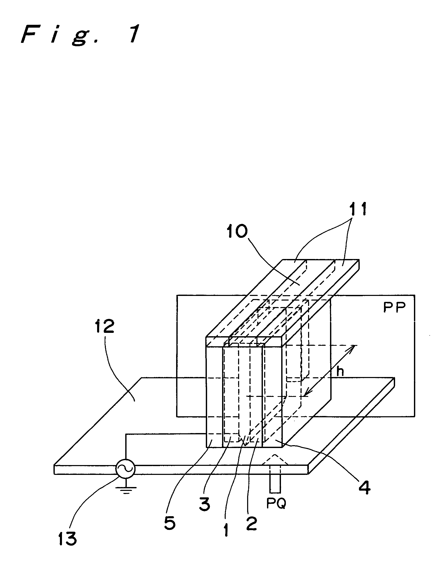
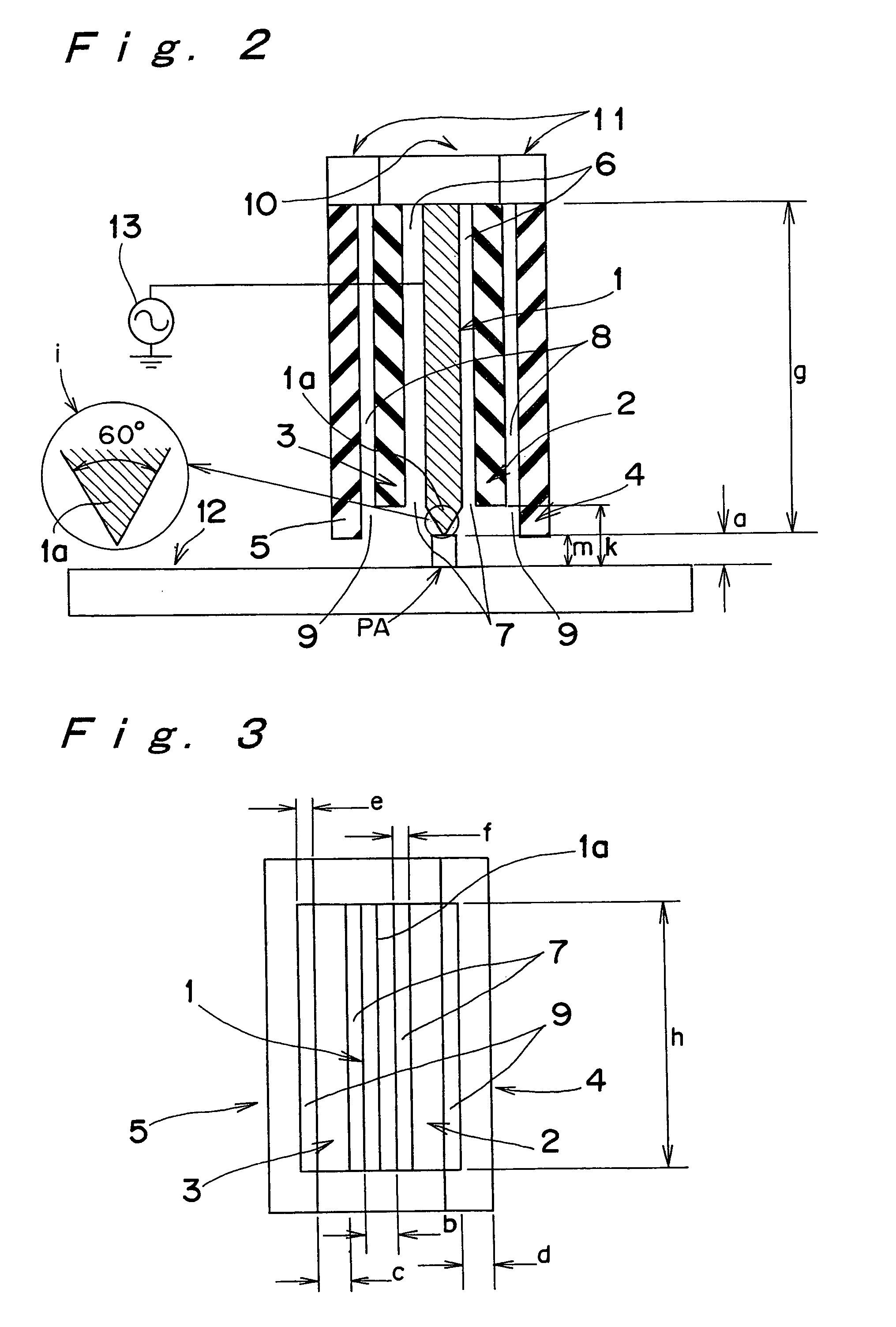
[0080]FIG. 1 shows a perspective view of a plasma processing apparatus including a plasma source equipped with a plate-shaped electrode 1 employed in the first embodiment of the present invention, in which a triangular-shaped taper portion (acute-angle portion) 1a having a thicknesswise symmetrical taper portion is provided at its lower end (an end portion on one side confronting the processing object [object to be processed]). FIG. 2 shows a sectional view taken along the plane PP of FIG. 1. Also, FIG. 3 is a plan view as viewed in a PQ direction of FIG. 1, showing the surface having the taper portion 1a of the plate-shaped electrode 1.

[0081]Referring to FIGS. 1 to 3, rectangular-parallelopiped plate-shaped insulators 2, 3 and C- or bracket([)-shaped, generally rectangular-parallelopiped plate-shaped insulators 4, 5 are disposed at positions where those are parallel to the plate-shaped electrode 1 having ...

third embodiment

[0087]As a third embodiment still different from FIG. 6, it is also possible, as shown in FIG. 11, that the plate-shaped insulators 4, 5 have two lengthwise discharge-control gas exhaust ports 15, respectively, which are provided at positions distant from each other by a specified distance h3 in the lengthwise direction of the plate-shaped electrode 1 and each of which extends from the plate-shaped electrode 1-side over the discharge-gas gas exhaust ports 7 up to near the discharge-control-gas gas exhaust ports 9. By jetting out through the lengthwise discharge-control gas exhaust ports 15 a discharge control gas of the same kind as the gas assigned to the gas exhaust port 9 located farther from the plate-shaped electrode 1, it becomes possible to suppress the etching rate at both ends of the taper portion 1a of the plate-shaped electrode 1. Furthermore, the discharge control gas to be jetted out through the lengthwise discharge-control gas exhaust ports 15 may also be given by a di...

fourth embodiment

[0110]The fourth embodiment according to the present invention is first explained below with reference to FIGS. 12A to 15D.

[0111]FIGS. 12A to 12C show a plasma processing apparatus according to the fourth embodiment, where FIG. 12A is a partly-cross-sectional front view of the plasma processing apparatus, FIG. 12B is a partly-cross-sectional side view of the apparatus, and FIG. 12C is an enlarged view of a part of FIG. 12A.

[0112]Referring to FIG. 12A, in a sealable vacuum chamber 301 formed of an insulator, metal, or semiconductor, a plate-shaped first electrode 302 and a plate-shaped second electrode 303 are disposed so as to face each other, and dielectric plates 304, 305 each formed of, for example, a 1 mm thick ceramic or alumina plate or the like are disposed in close contact with the first electrode 302 and the second electrode 303, respectively. The dielectric plates 304, 305 have grooves 306, 307, respectively, formed so as to each have a width of 20 mm and a step gap of 0.0...


PUM

PropertyMeasurementUnit
frequencyaaaaaaaaaa
thicknessesaaaaaaaaaa

Abstract

In a state that a plate-shaped insulator is disposed adjacent to a plate-shaped electrode, a discharge gas containing an inert gas is supplied to a vicinity of a processing object from one gas exhaust port located nearer from the plate-shaped electrode, out of at least two-line gas exhaust ports which are disposed around the plate-shaped electrode and which are formed so as to be surrounded by the plate-shaped insulator and moreover which are different in distance to the plate-shaped electrode from each other, while a discharge control gas is supplied from the other gas exhaust port to the vicinity of the processing object. Simultaneously with the supply of the gases, electric power is supplied to the plate-shaped electrode or the processing object, by which plasma processing of the processing object is carried out. Thus, plasma processing method and apparatus capable of processing for desired fine linear portions with high precision are provided.

Description

BACKGROUND OF THE INVENTION[0001]The present invention relates to plasma processing method and apparatus for performing plasma processing by using a plasma on, for example, processing objects (objects to be processed) such as a substrate having a thin film formed on its surface or processing objects coated with various types of films so that desired fine linear portions are worked with high precision, or for performing plasma processing by using a plasma on the surface of various processing objects so that a thin film is deposited thereon.[0002]In general, when an object to be processed typified by a substrate with a thin film formed thereon is subjected to a patterning process, a resist process is used. FIGS. 7A to 7D show one example of the process. In FIGS. 7A to 7D, first, photosensitive resist 14 is applied onto the surface of an object 12 to be processed (FIG. 7A). Next, the resist 14 is exposed to light with an exposer and thereafter developed, by which the resist 14 can be p...

Claims


Application Information

Patent Timeline
Patent Type & Authority Patents(United States)
IPC IPC(8): B23K10/00H01L21/3065H01J37/32
CPCH01J37/32009H01J37/32532H01J37/3244H01L21/3065
Inventor YASHIRO, YOICHIROOKUMURA, TOMOHIROKIMURA, TADASHISAITOH, MITSUO
Owner PANASONIC CORP
Why Eureka
Try Eureka