Scan flip flop, semiconductor device, and production method of semiconductor device
a flip flop and flip flop technology, applied in the field of flip flops, can solve the problems of increasing the operation speed, reducing the area, and reducing the power consumption, so as to reduce the number of mos transistors and the speed of operation.
- Summary
- Abstract
- Description
- Claims
- Application Information
AI Technical Summary
Benefits of technology
Problems solved by technology
Method used
Image
Examples
embodiment 1
[0064](Embodiment 1)
[0065]In the first place, embodiment 1 of the present invention is described.
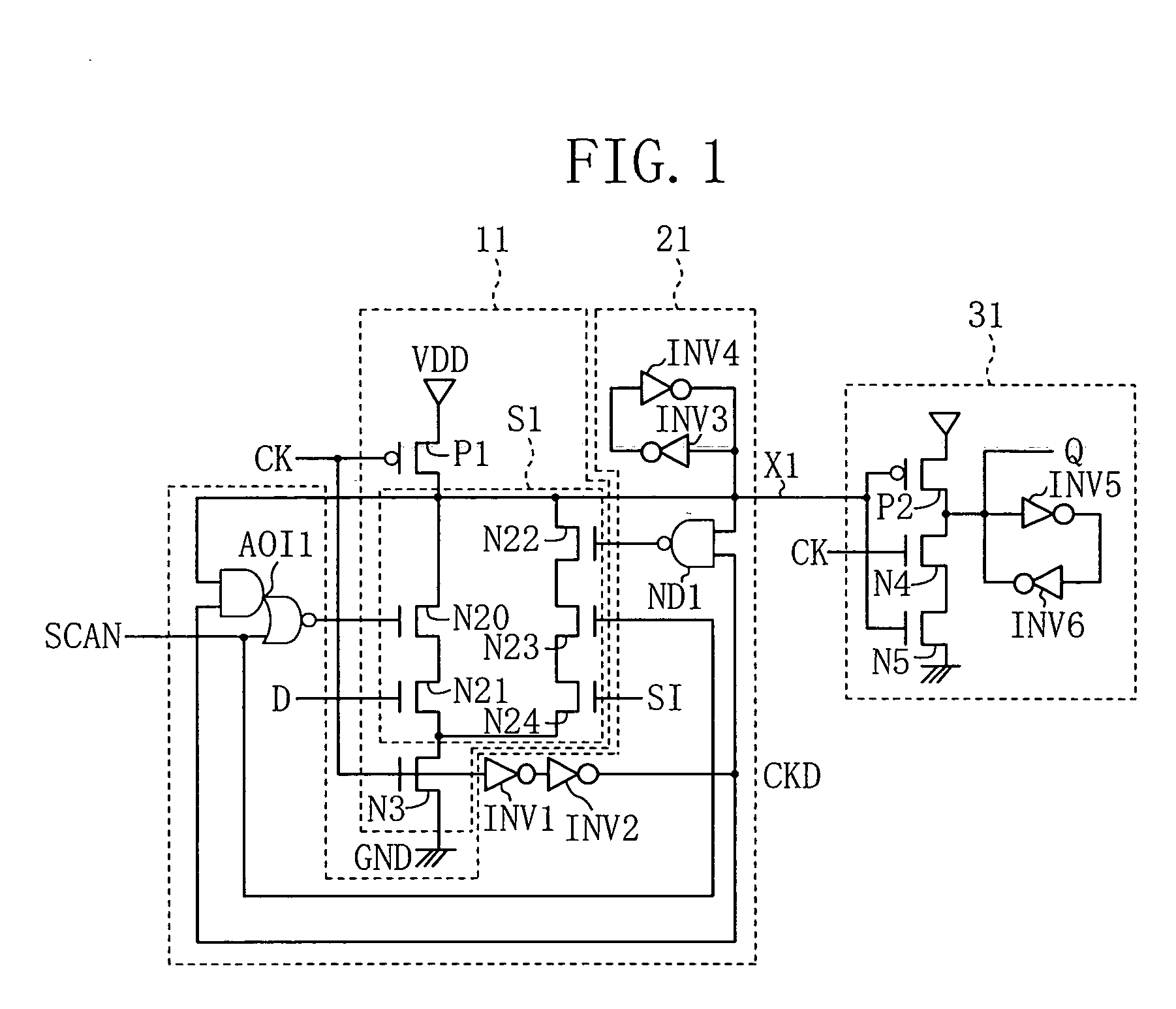
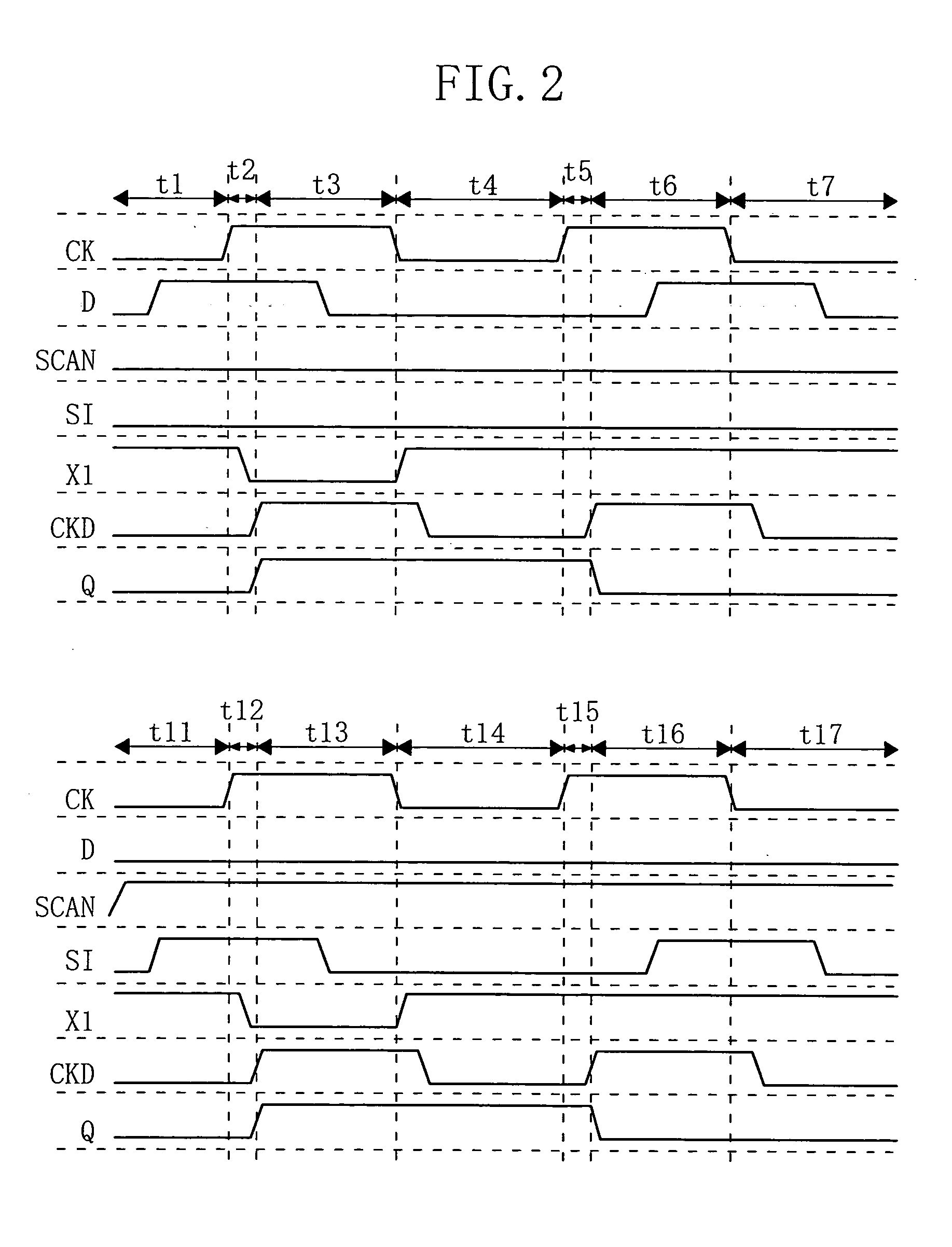
[0066]FIG. 1 is a circuit diagram showing a scan flip flop circuit according to embodiment 1 of the present invention. FIG. 2 is a timing chart which illustrates an operation of the scan flip flop circuit.
[0067]In FIG. 1, “D” denotes a data signal, “CK” denotes a clock signal, “SI” denotes a test input signal, “SCAN” denotes a test selection signal (including a data signal, a clock signal, a test input signal, first logic information of a test selection signal), “Q” denotes an output signal, “VDD” denotes a VDD power supply, and “GND” denotes a GND potential.
[0068]Reference numeral “AOI1” denotes an AND / OR inverter circuit which outputs an operation result of NOR logic of the output of a 2-input AND circuit and test selection signal SCAN. Reference numeral “ND1” denotes a 2-input NAND circuit. Reference numerals “N20” to “N24” denote nMOS transistors. A series connection of the nMOS tran...
embodiment 2
[0082](Embodiment 2)
[0083]Hereinafter, a scan flip flop according to embodiment 2 of the present invention is described with reference to the drawings.
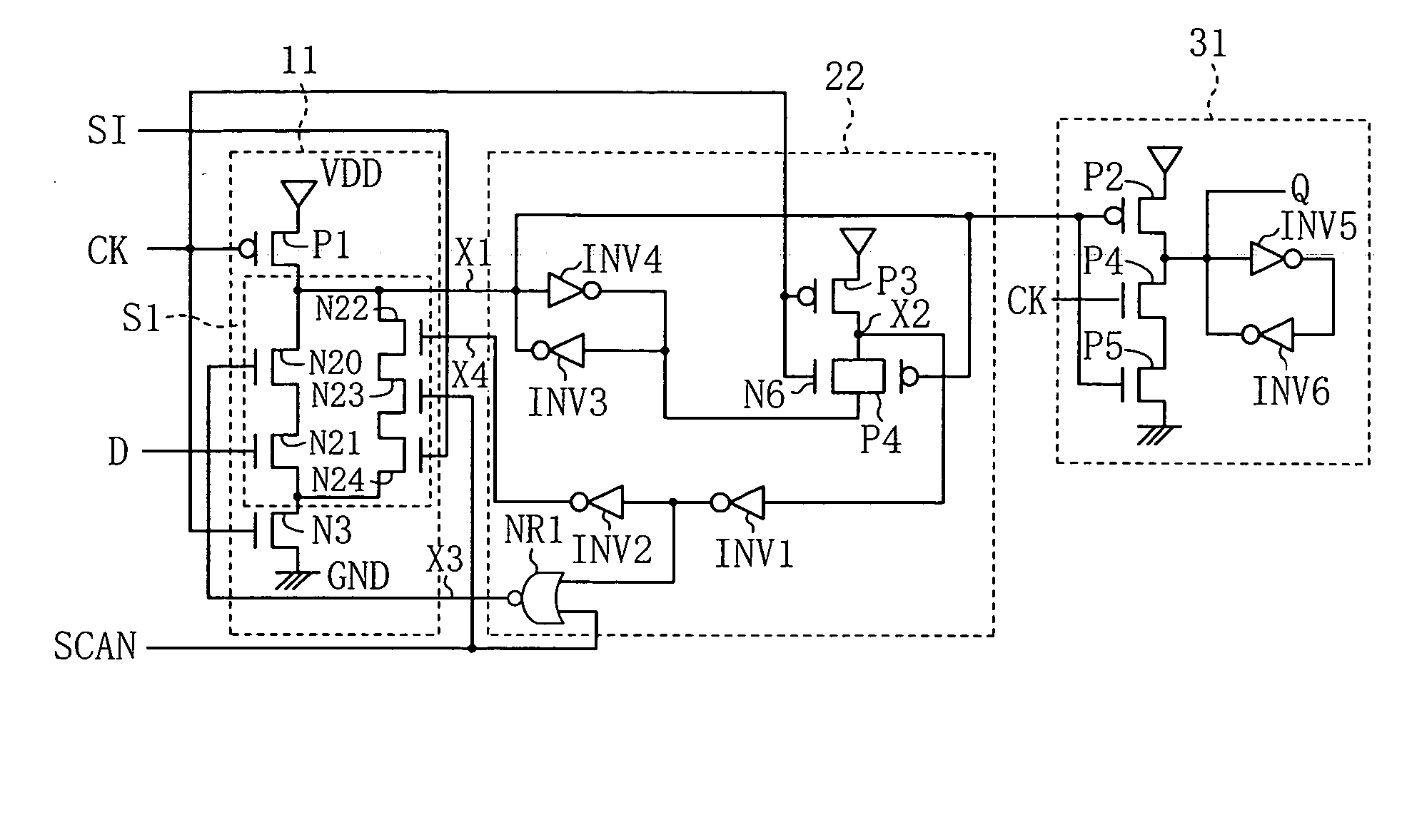
[0084]FIG. 3 is a circuit diagram showing a scan flip flop circuit according to embodiment 2. FIG. 4 is a timing chart which illustrates an operation of the scan flip flop circuit.
[0085]In the scan flip flop shown in FIG. 3, the input section 11 at the input side (including the pMOS transistor P1 and the nMOS transistors N20 to N24 and N3) and the output section 31 at the output side (including the pMOS transistor P2, the nMOS transistors N4 and N5, and the inverter circuits INV5 and INV6) have the same structures as shown in FIG. 1 in embodiment 1, and therefore, the descriptions thereof are omitted.
[0086]In embodiment 2, in the selector circuit S1 formed by the five nMOS transistors N20 to N24, a control section 22 for generating control signals which are input to the gate of the nMOS transistor N20 (third node X3 in FIG. 3) and the...
embodiment 3
[0103](Embodiment 3)
[0104]FIG. 5 is a circuit diagram showing a scan flip flop according to embodiment 3. FIG. 7 is a timing chart which illustrates an operation of the scan flip flop. It should be noted that, in embodiment 3, the same circuit components as those shown in the circuit diagrams of FIGS. 1 and 3 in embodiments 1 and 2 are denoted by the same reference numerals, and the descriptions thereof are omitted.
[0105]In embodiment 3, an input section 12, which includes the pMOS transistor P1, nMOS transistors N3, N20 to N24, is different from the input section 11 of embodiment 2 in that a selector circuit S1 formed by the nMOS transistors N20 to N24 is connected between the nMOS transistor N3 and the GND potential.
[0106]In the structure of FIG. 3 (embodiment 2), the nMOS transistor N6 and the pMOS transistor P4 are connected in series to the pMOS transistor P3 to constitute a transmission gate. However, in FIG. 5 of embodiment 3, only the nMOS transistor N6 is connected in serie...
PUM
 Abstract
Description
Claims
Application Information


