
Test method and architecture for circuits having inputs

Inactive Publication Date: 2007-01-02
NAT SCI COUNCIL
View PDF17 Cites 9 Cited by
  • Summary
  • Abstract
  • Description
  • Claims
  • Application Information

AI Technical Summary

Benefits of technology

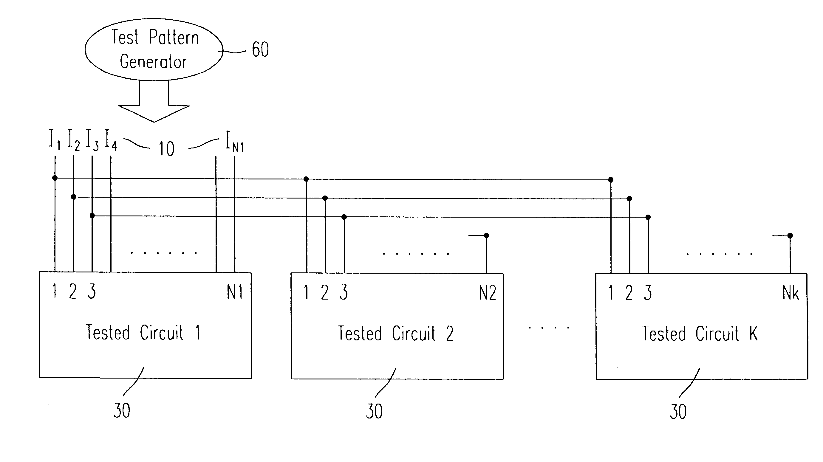
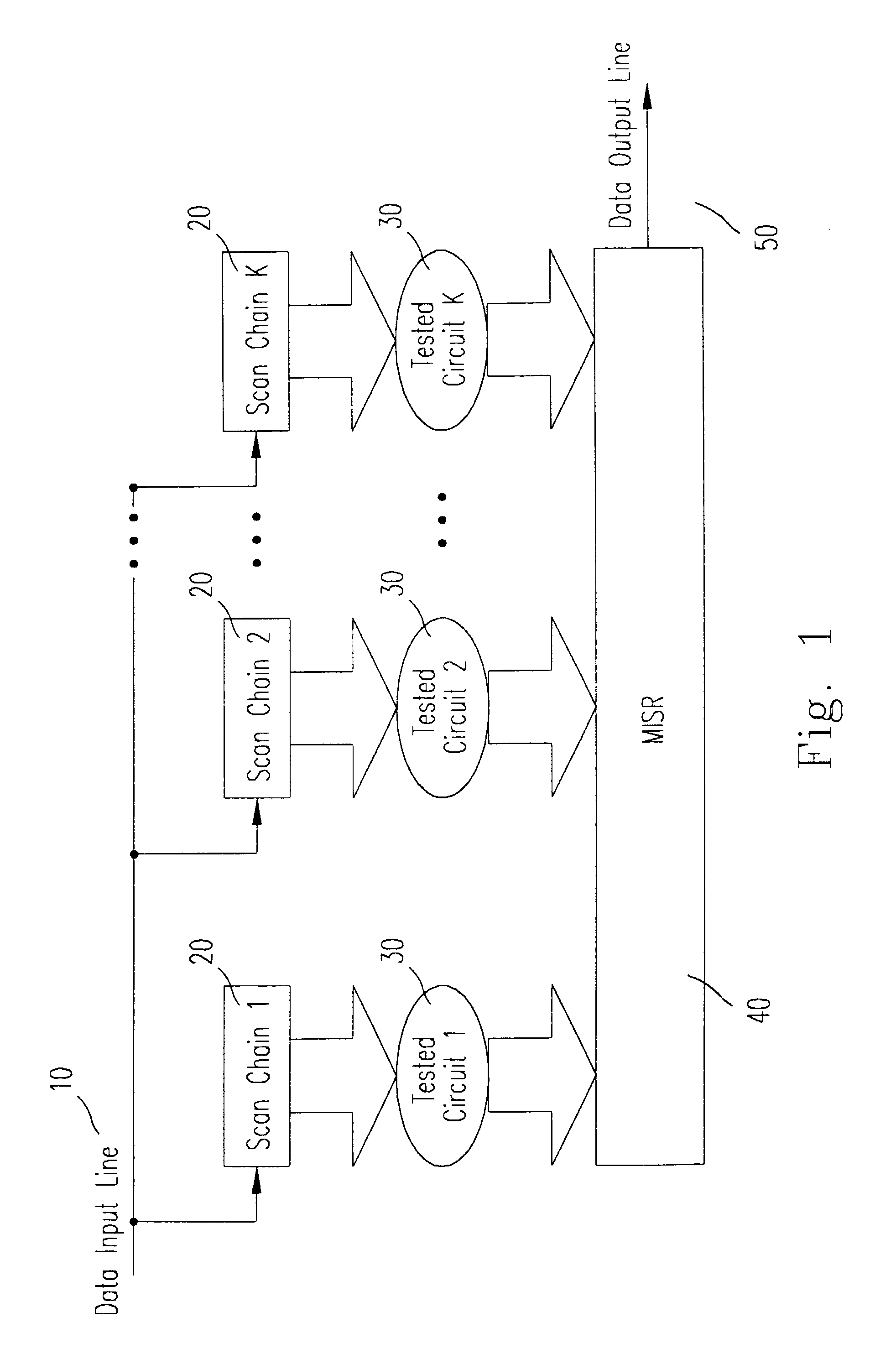
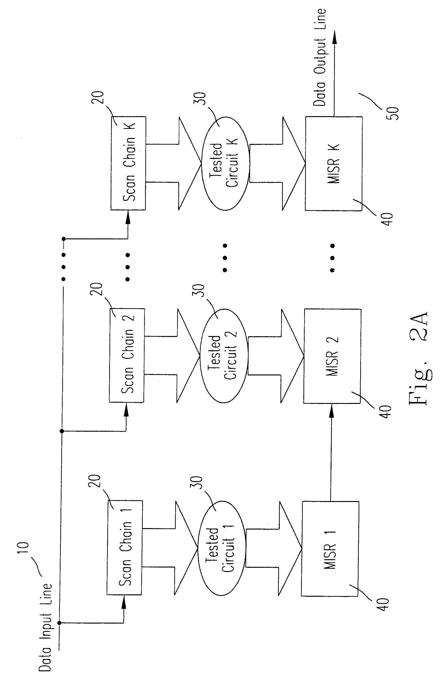
[0006]The present invention includes a method to resolve the above problems and an architecture to implement the invented method. The invention allows the use of one single input to provide test data to multiple scan chains of a plurality of circuits while the test time is still very close to that for the conventional multiple scan chain techniques. The fault coverage with the present invention is the same as that using a single scan chain or multiple scan chains but the required test volume of the present invention is much less than the single or multiple scan methods. A virtual circuit construction technique is invented that can assist the automatic test pattern generation procedure to generate the common test patterns that can be broadcast to all circuits under test with no fault coverage loss. Since only one data input is required to provide test input data, the present invention can be easily applied to the boundary scan technique, which is a widely-accepted industry standard for chip level test interface, also known as IEEE Std. 1149.1. The invention can be applied to both combinational or sequential circuits. For combinational circuits it is assumes that the inputs of the combinational circuits can be chained together to form a scan chain and hence the required test input data can be scanned in. For sequential circuits, the internal storage elements are assumed to be constructed into scan chains while the inputs can either be a part of the scan chains or remain as primary inputs without scan chains to chain them together.

Problems solved by technology

When a scan chain includes too many scan elements, however, the required test time will be relatively long.
Since the present peripheral scan architecture only permits a data input line and a data output line, it cannot effectively support the multiple scan chain test design.

Method used


Image

  • Test method and architecture for circuits having inputs
  • Test method and architecture for circuits having inputs
  • Test method and architecture for circuits having inputs

Examples


Embodiment Construction

[0055]The present invention is based on the recognition that upon proceeding the automatic test pattern generation (ATPG), a replacing test pattern optimally taking advantages of compatibilities of required test patterns of respective circuits without a lowered fault coverage is obtained. This differs from the conventional test pattern compression technique in that the former compression technique is directed to handle a single tested circuit whereas the present invention aims to deal with a plurality of tested circuits obtaining test data through a single data line. In order to better interpret the present invention, we use two tested circuits 1 and 2.

[0056]In the beginning of proceeding the automatic test pattern generation, a random test pattern is used to detect the fault until a certain fault coverage is reached. After most of faults are detected by the random test pattern, a deterministic test pattern is specially provided to deal with the rest detectable faults. If test patte...


PUM


Abstract

A test method for a plurality of circuits respectively having inputs for greatly reducing the required test time and the control circuit complexity is provided. The method includes steps of providing a set of test patterns for detecting a characteristic of the circuits, providing a common data line, and electrically connecting the circuit inputs to the common data line so that the test pattern can be broadcasted to the circuits through the common data line. The present invention also provides an architecture for implementing such method.

Description

FIELD OF THE INVENTION[0001]The present invention relates to a test method or architecture, and more particularly to one for circuits having inputs.BACKGROUND OF THE INVENTION[0002]The scan based design is one of the most acceptable methods in the industry for testable design, and is mainly aimed in greatly reducing the complexity of the automatic test pattern generation (ATPG) process. When a scan chain includes too many scan elements, however, the required test time will be relatively long. Although the multiple scan chain design is one of measures which can effectively decrease the test time that the scan type circuit requires, the control circuit therefor normally is more complex than that for the single scan chain design and the required additional pin number will proportionally increase with the number of the scan chains.[0003]S. Narayanan et al. disclosed in the article entitled “Asynchronous Multiple Scan Chains” for IEEE VLSI Test Symposium in 1995 that multiple scan chains...

Claims


Application Information

Patent Timeline
IPC IPC(8): G01R31/28G01R31/3185
CPCG01R31/318583G01R31/318563G01R31/318547
Inventor LEE, KUEN-JONGCHEN, JIH-JEENHUANG, CHENG-HUA
Owner NAT SCI COUNCIL
Learn More