Electrode for lithium secondary battery and lithium secondary battery

a lithium secondary battery and lithium secondary battery technology, applied in the direction of negative electrodes, electrode manufacturing processes, cell components, etc., can solve the problems of low discharge cycle characteristics, large volume expansion and shrinkage during charge-discharge reaction, and silicon not being put into practical use, etc., to achieve satisfactory maintenance and improve discharge cycle characteristics

Inactive Publication Date: 2007-01-09
SANYO ELECTRIC CO LTD
View PDF13 Cites 20 Cited by
  • Summary
  • Abstract
  • Description
  • Claims
  • Application Information

AI Technical Summary

Benefits of technology

[0022]It is preferable that the content of the element in the thin film is not more than 17 atomic %. The reason for this is not clear, but it is considered that when the content of the element in the thin film is too large, aggregation of the element easily occurs, and this easily causes the pulverization of the active material layer, and thus the effect for improving the cycle characteristics is reduced.
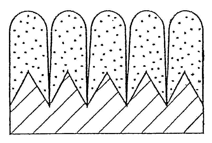
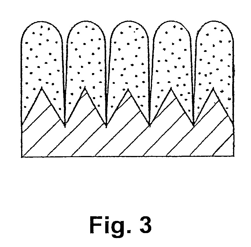
[0023]It is preferable that the thin film of the present invention is separated into columns by gaps formed in its thickness direction as illustrated in FIG. 3. Since gaps exist around the columnar portions, and the gaps absorb a stress generated by expansion and contraction of the thin film during the charge-discharge cycles, and the generation of a stress for falling off the thin film from the current collector can be suppressed. Therefore, an adhesion state of a bottom portion of the columnar portion and the current collector can be maintained satisfactorily.
[0024]In addition, it is preferable that at least a not less than half portion of the thickness of the thin film is separated into the columns by the gaps in the thickness direction of the thin film.
[0025]Further, in the case where an uneven portion is formed on the surface of the thin film and the gaps, in which a recessed portion of the uneven portion is its end, is formed on the thin film, the gaps may be formed so that the columnar portion includes at least one convex portion on the thin film surface. In this case, the gaps may be formed so that the columnar portion includes a plurality of convex portions.
[0026]The gaps formed on the thin film may be formed by charge and discharge after initial charge and discharge. In this case, for example, the uneven portion is formed on the surface of the thin film before charge and discharge, and the gaps, in which a recessed portion of the uneven portion on the surface of the thin film is its end, is formed by charge and discharge after initial charge and discharge, and these gaps may separate the thin film into the columns.
[0027]The uneven portion on the surface of the thin film may be formed correspondingly to an uneven portion on the surface of the current collector as a ground layer. Namely, the current collector having the uneven portion on its surface is used and the thin film is formed thereon, so that the uneven portion can be provided on the surface of the thin film.

Problems solved by technology

However, since silicon is alloyed with lithium to store, volume expansion and shrinkage during charge-discharge reaction are large.
For this reason, the active material is pulverized and separated from a current collector, so that the charge-discharge cycle characteristics are not good and thus silicon is not put into practical use.
In order to solve the above problem, silicon as the active material is attempted to be improved by doping impurity into silicon (Japanese Patent Laid-Open No. 10-199524 (1998)), and by using alloy powder of silicon and a different element (Japanese Patent Laid-Open No. 2000-243389), but sufficient results are not yet obtained.
However, a capacity retention rate is improved by making silicon into an intermetallic compound, but the discharge capacity after cycles is not substantially improved.

Method used


Image

  • Electrode for lithium secondary battery and lithium secondary battery
  • Electrode for lithium secondary battery and lithium secondary battery
  • Electrode for lithium secondary battery and lithium secondary battery

Examples


experiment 1

[0060](Experiment 1)

[0061][Manufacturing of Negative Electrode]

[0062]Electrolytic copper foil (thickness: 18 μm, surface roughness: Ra=0.188 μm) was used as a current collector, and a thin film was formed on the electrolytic copper foil by an RF sputtering method. As the thin film, a silicon-cobalt thin film, a silicon-chromium thin film and a silicon thin film were formed. As the silicon-cobalt thin film, five kinds of thin films in which their cobalt content are different from one another were formed.

[0063]The sputtering conditions were such that sputter gas (Ar) flow rate: 10 sccm, a substrate temperature: room temperature (without heating), reactive pressure: 0.665 Pa (5×10⁻³ Torr) and a high frequency power: 500 W. A single crystalline silicon target (diameter: 4 in (100 mm)) was used as a target, and as for fabricating samples which contain cobalt as a different element, cobalt (Co) chips were arranged on the silicon (Si) target, and as for fabricating samples which contain ch...

experiment 2

[0083](Experiment 2)

[0084]Similarly to the experiment 1, thin films were formed on the electrolytic copper foil by an RF sputtering method. As the thin film, a silicon-zinc thin film, a silicon-iron thin film, a silicon-nickel thin film, a silicon-zirconium thin film, a silicon-silver thin film, a silicon-manganese thin film, a silicon-molybdenum thin film, a silicon-tantalum thin film, a silicon-niobium thin film, a silicon-titanium thin film, a silicon-tungsten thin film and a silicon-vanadium thin film were formed.

[0085]As for a target, similarly to the experiment 1, the chips made of the above different elements were arranged on the single crystalline silicon target. The sizes and numbers of the chips are shown in Table 3.

[0086]The obtained thin films were subjected to the Raman spectroscopy analysis, so that it was confirmed that they were thin films comprising amorphous silicon as a main component.

[0087]Similarly to the experiment 1, the lithium secondary batteries were manufa...

experiment 3

[0093](Experiment 3)

[0094]The electrolytic copper foil (thickness: 18 μm, surface roughness: Ra=0.188 μm) was used as the current collector, and thin films were formed on the electrolytic copper foil by the sputtering method using DC pulse discharge. As the thin films, a silicon-cobalt thin film, a silicon-zinc thin film, a silicon-iron thin film and a silicon-zirconium thin film were formed.

[0095]The sputtering conditions were such that a sputter gas (AR) flow rate: 85 sccm, a substrate temperature: room temperature (without heating), reactive pressure: 0.532 Pa (4×10⁻³ Torr), a DC pulse frequency: 100 kHz, a pulse width: 1.696 μs and an applying power: 1300 W. The thin films were formed on the electrolytic copper foil of 175 mm×400 mm so that their thickness becomes about 6 μm.

[0096]As the target, silicon alloy targets of 35 cm×20 cm, which were obtained by mixing respective elements including cobalt, zinc, iron and zirconium with silicon and sintering them, were used. The type an...


PUM

PropertyMeasurementUnit
surface roughness Raaaaaaaaaaa

Abstract

An electrode for lithium secondary battery having a current collector and, deposited thereon, a thin film comprising silicon as a main component, characterized in that the thin film comprising silicon contains at least one of the elements belonging to the groups IIIa, Iva, Va, VIa, VIIa, VIII, Ib and IIb in the fourth, fifth and sixth periods of the Periodic Table (exclusive of copper (Cu)) at least in the surface portion thereof.

Description

BACKGROUND OF THE INVENTION[0001]1. Field of the Invention[0002]The present invention relates to an electrode for lithium secondary battery and lithium secondary battery using this.[0003]2. Related Art[0004]In recent years, development in lithium secondary batteries has been conducted enthusiastically. As for the lithium secondary battery, its battery characteristics such as charge-discharge voltage, charge-discharge cycle life characteristic and storage characteristic are greatly influenced by electrode active materials to be used.[0005]In the electrode active materials capable of lithium storage and release, silicon is variously examined, since silicon can store lithium by being alloyed with lithium so that its theoretical capacity is large. However, since silicon is alloyed with lithium to store, volume expansion and shrinkage during charge-discharge reaction are large. For this reason, the active material is pulverized and separated from a current collector, so that the charge-d...

Claims


Application Information

Patent Timeline
Patent Type & Authority Patents(United States)
IPC IPC(8): H01M4/58H01M4/66C22C28/00H01M4/134H01M4/1395H01M4/36H01M4/38H01M4/70H01M10/05
CPCH01M4/0404H01M4/364H01M4/38H01M4/386H01M4/58H01M4/661H01M10/052H01M2004/027Y02E60/10
Inventor OHSHITA, RYUJIOTA, TAEKOKAMINO, MARUOTARUI, HISAKIFUJIMOTO, MASAHISAFUJITANI, SHINSAYAMA, KATSUNOBU
Owner SANYO ELECTRIC CO LTD
Why Eureka
Try Eureka