Systems and apparatus for digital control of bias for transistors

a technology of transistors and digital control, applied in the field of power amplifiers, can solve the problems of high labor costs and high parts costs

Inactive Publication Date: 2007-01-16
SILICON LAB INC
View PDF9 Cites 14 Cited by
  • Summary
  • Abstract
  • Description
  • Claims
  • Application Information

AI Technical Summary

Problems solved by technology

This is an expensive approach both in terms of parts costs and labor costs.

Method used


Image

  • Systems and apparatus for digital control of bias for transistors
  • Systems and apparatus for digital control of bias for transistors
  • Systems and apparatus for digital control of bias for transistors

Examples


Embodiment Construction

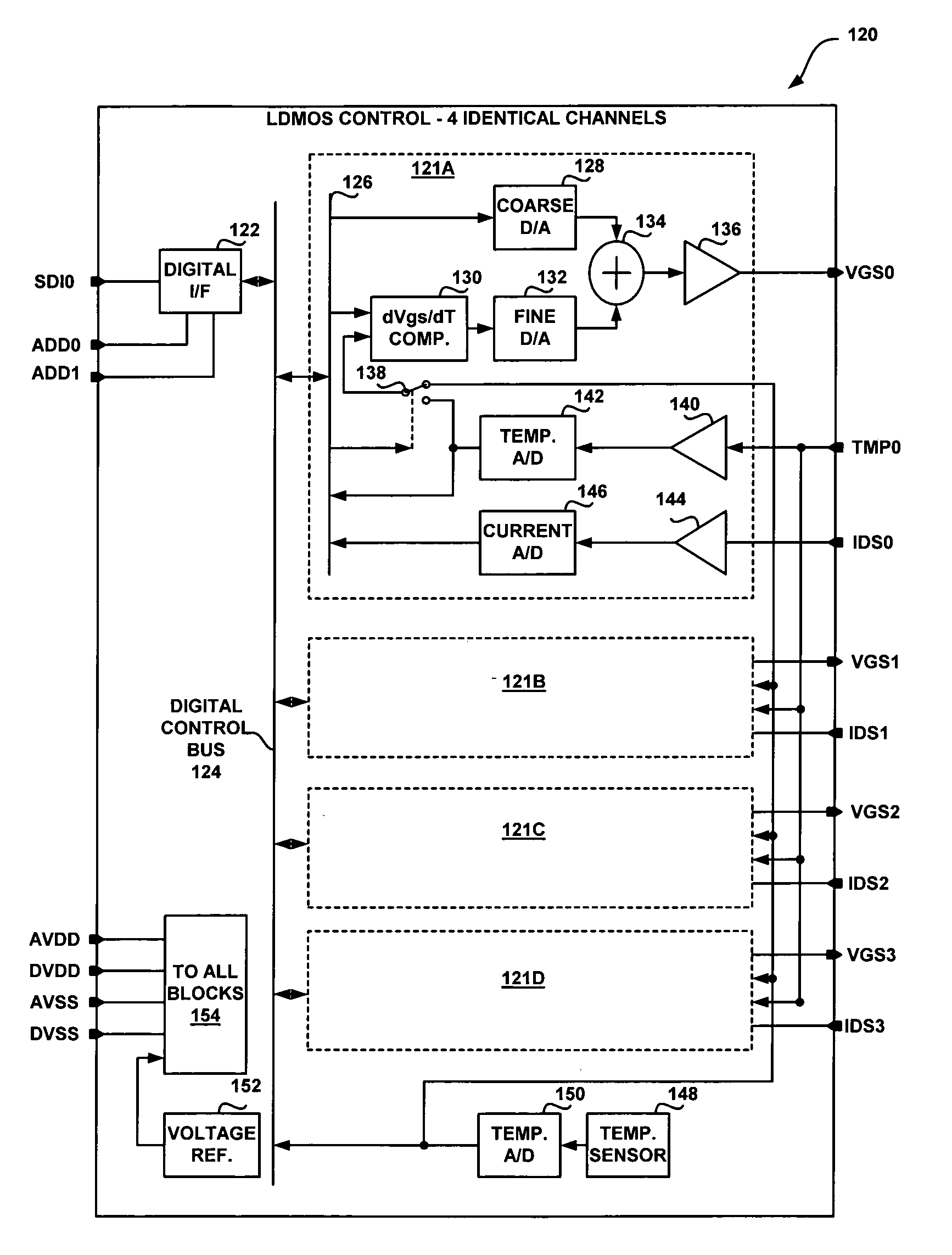
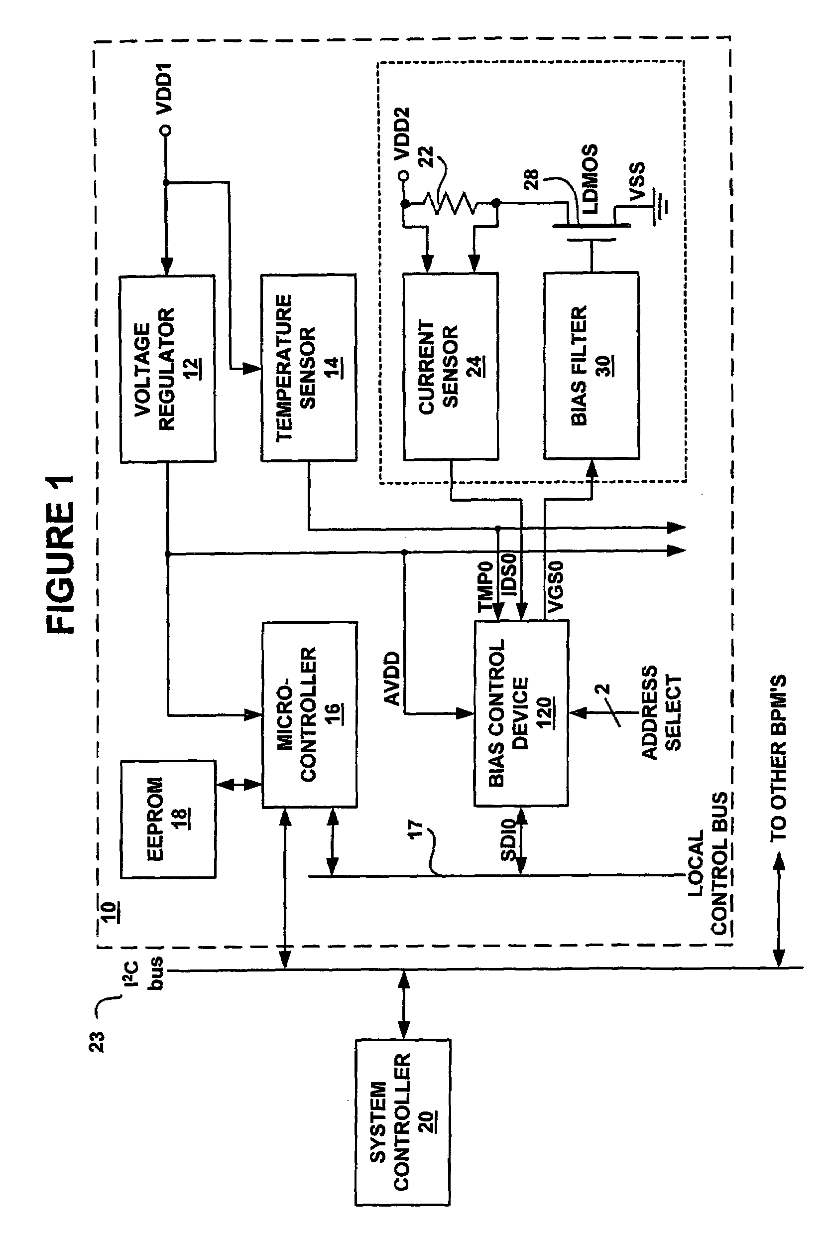
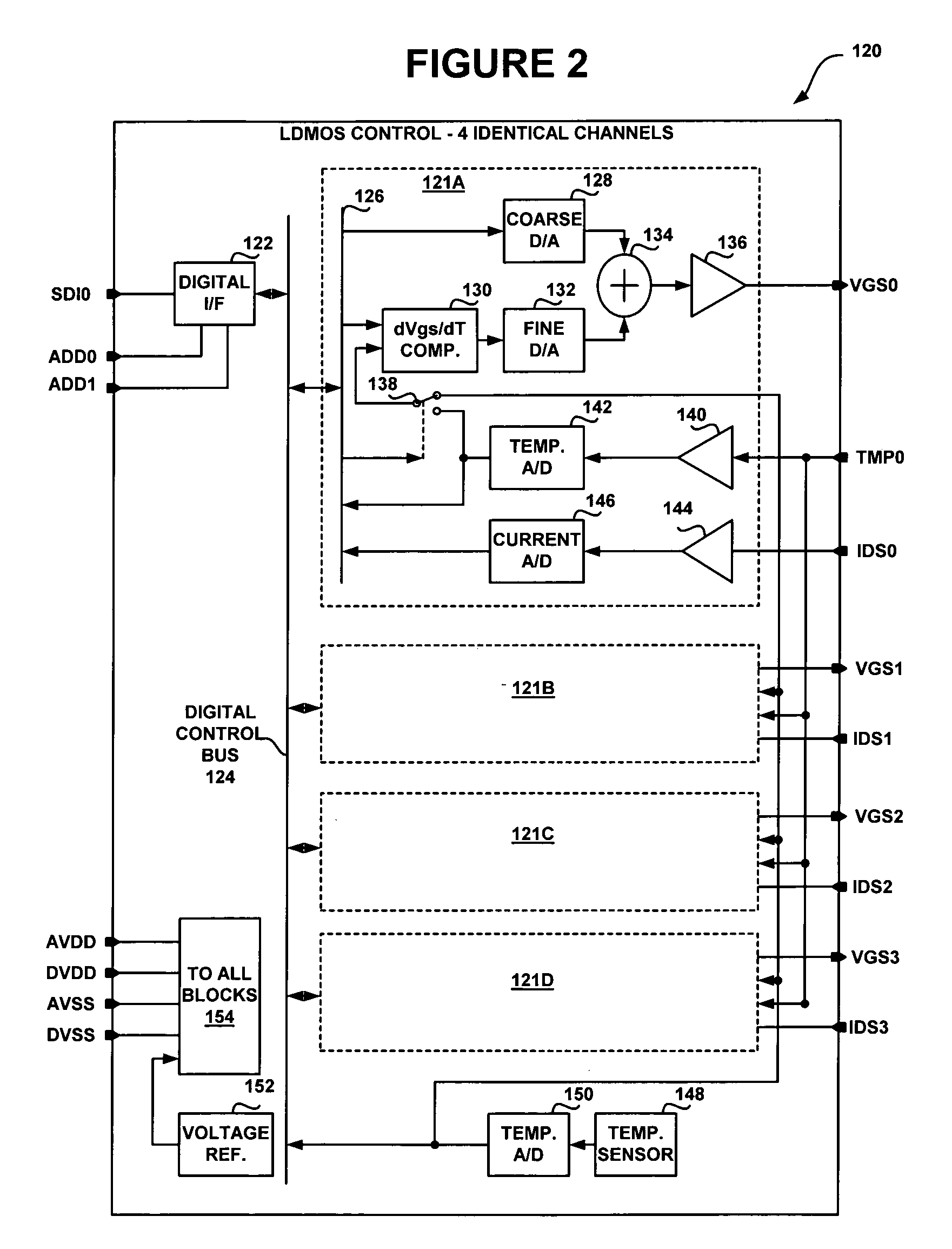
[0012]The present invention is directed toward a method and apparatus for digital control of biasing for power amplifiers, whereby the biasing of a transistor may be automatically adjusted. It is useful to automatically adjust biasing to meet the requirements of a variety of applications, such as for reduced power or to accommodate pre-distortion of the amplified signal. Similarly, the biasing may be automatically adjusted to adapt to changes in the characteristics of the transistors, such as due to temperature changes or aging.

[0013]In one embodiment of the present invention, a bus control device according to the present invention is configured to generate temperature compensated gate bias voltage for LDMOS transistors used in RF power amplifiers. In this embodiment, a number of transistors controlled by the bus control device can each have different parameters programmed via a single interface bus, such as a single-wire serial digital interface bus. Furthermore, in this embodiment...


PUM


Abstract

The present invention is directed toward a system and apparatus for digitally controlling a bias control signal for at least one transistor. The present invention provides for software writable registers that control the bias control signal. The present invention further provides for the bias control signal to be temperature compensated based upon a temperature signal and a temperature profile stored in software writable registers. The present invention further provides for software control of the initialization and configuration of the bias control signal through stored program control of the values in the software writable registers.

Description

CROSS-REFERENCES TO RELATED APPLICATIONS[0001]This application claims priority to co-pending provisional patent application No. 60 / 283,413 filed Apr. 12, 2001 and co-pending provisional patent application No. 60 / 352,903 filed Jan. 28, 2002, both of which are incorporated by reference in their entirety for all purposes.FIELD OF THE INVENTION[0002]The present invention relates to power amplifiers. More specifically, it relates to a method and apparatus for digital control of biasing for power amplifiers.BACKGROUND OF THE INVENTION[0003]Many systems, such as wireless telephone base stations, employ multiple power transistors, such as LDMOS (Laterally Diffused MOS) transistors, to amplify a signal for transmission, e.g. a radio frequency (RF) signal. Typically, the biasing for the power transistors is implemented using discrete devices that must be hand tuned for the particular application and the characteristics of the particular transistors employed. This is an expensive approach both...

Claims


Application Information

Patent Timeline
Patent Type & Authority Patents(United States)
IPC IPC(8): G05F1/10
CPCG01R31/3167H03K2005/00143
Inventor NAULEAU, JEAN-LUCERDELYI, JANOSMCCALPIN, WILLIAM H.
Owner SILICON LAB INC
Why Eureka
Try Eureka