Method of making a packaged semiconductor device

a semiconductor device and packaging technology, applied in semiconductor devices, semiconductor/solid-state device details, electrical equipment, etc., can solve the problems of increasing production complexity and cost, adding production time, complexity and cost, clip attachment, wire bonding or ribbon bonding steps, etc., to achieve cost saving, low cost, and thin device

Active Publication Date: 2007-01-23
CICLON SEMICON DEVICE
View PDF69 Cites 57 Cited by
  • Summary
  • Abstract
  • Description
  • Claims
  • Application Information

AI Technical Summary

Benefits of technology

[0008]From the foregoing, a packaged device is provided that can be manufactured in a low cost and very production friendly manner. The package itself lacks the complexity of prior art packages, providing a robust package and cost savings. Because the die is provided in a recessed area etched in a planar layer of conductive material, a very thin device is produced. Further, the leadframe is easily configured to accommodate any number of die sizes, quantity die, type of die and electrode configurations simply by etching a different recessed region patterned into a leadframe precursor. The process and package, therefore, are easily scalable to different I / O (input / output) and die configurations, providing consequent reductions in development costs and time as well as implementation times for new designs. Custom and expensive wire or clip bonding machinery as well as trimming and forming machinery are not needed.

Problems solved by technology

These trimming and forming steps and requisite machinery along with the solder or epoxy die attachment and wire bonding, ribbon bonding or clip bonding add to production time, complexity and cost.
While no post-encapsulation forming step is required to bend and shape the leads, the clip attachment, wire bonding or ribbon bonding and die attachment steps increase production complexity and cost.

Method used


Image

  • Method of making a packaged semiconductor device
  • Method of making a packaged semiconductor device
  • Method of making a packaged semiconductor device

Examples


Embodiment Construction

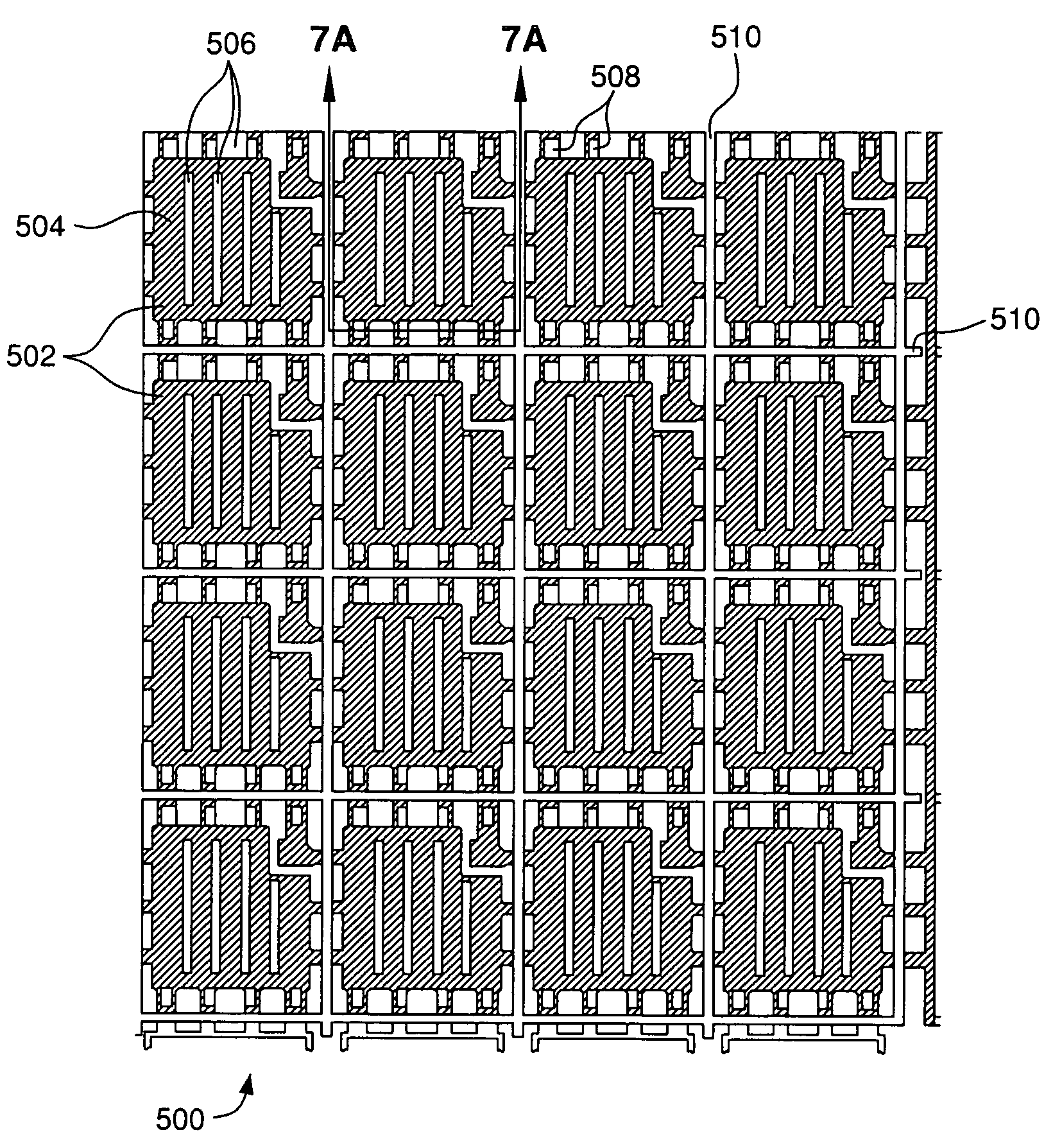
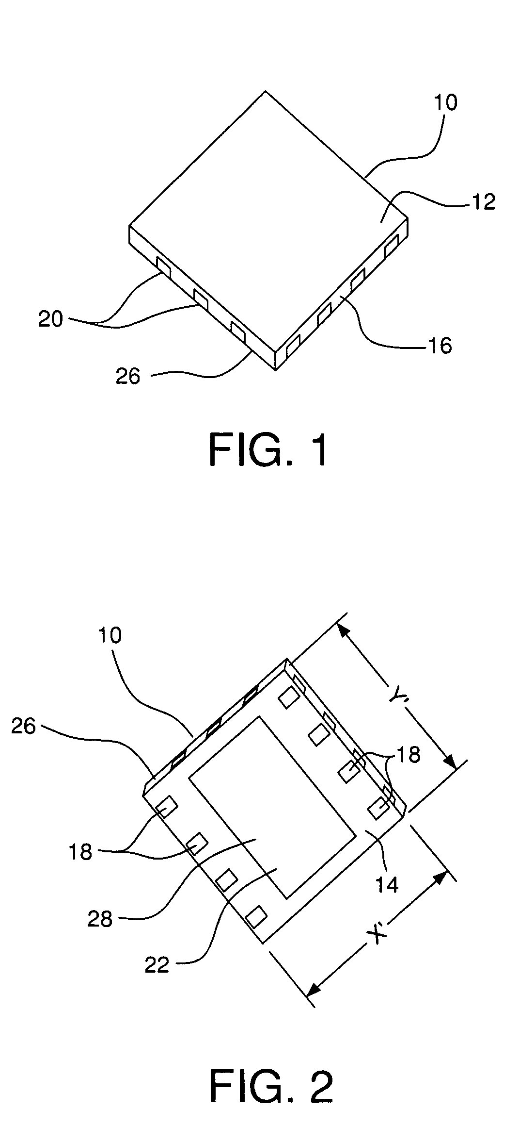
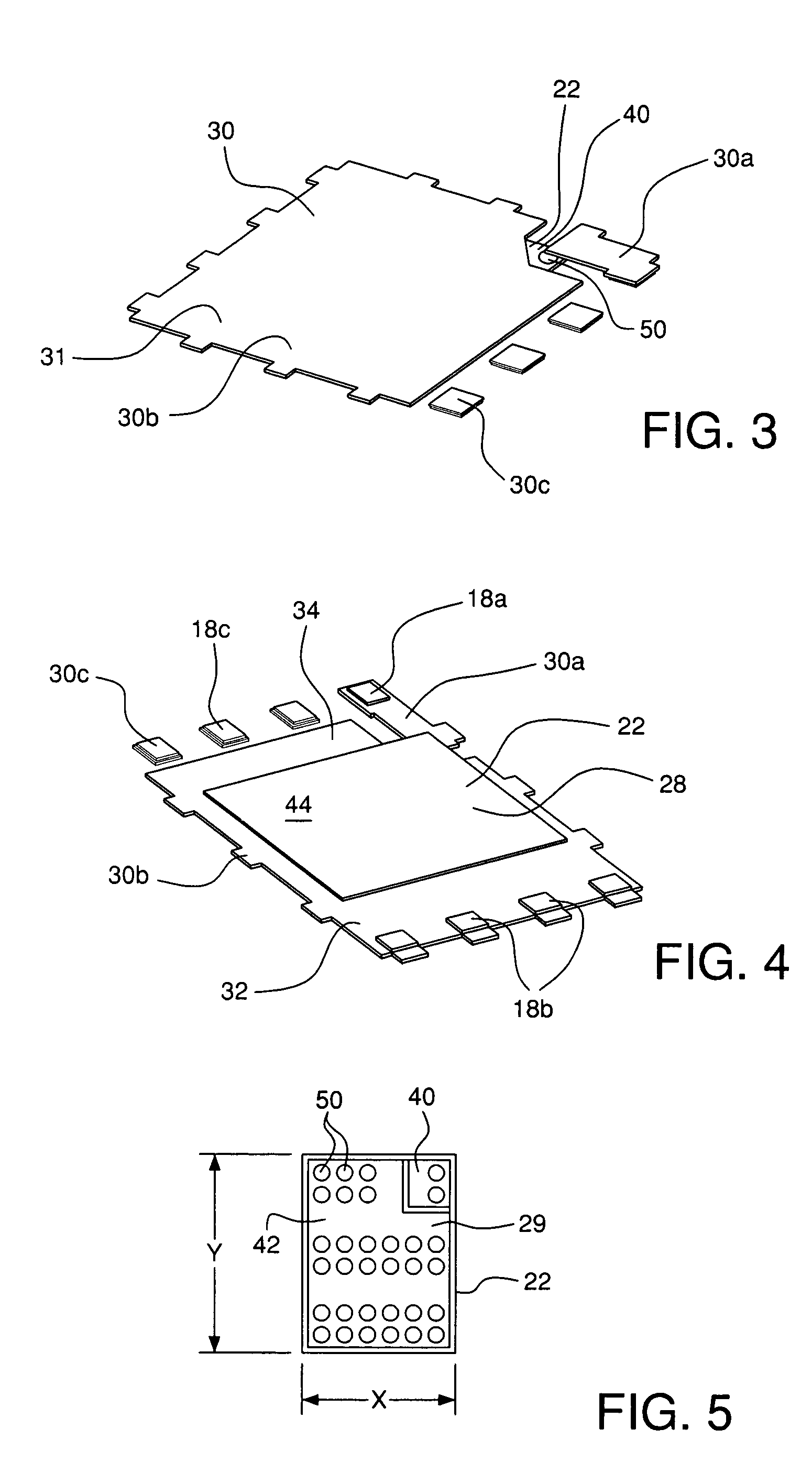
[0022]FIG. 1 is a top perspective view of a packaged semiconductor device 10, and FIG. 2 is a bottom perspective view of the device 10. Packaged device 10 has a planar top surface 12, a planar bottom surface 14 and side surfaces 16 generally orthogonal to the top and bottom surfaces 12, 14. As best seen in FIG. 2, the packaged device comprises a plurality of exposed lead contacts 18 which can comprise dummy lead contacts (i.e., contacts that are not internally electrically coupled to the semiconductor device) and any number of active lead contacts (i.e., contacts that are internally electrically coupled to the semiconductor device). Packaged device 10 includes a semiconductor die 22 having a bottom surface 28 having a bottom surface electrode exposed through encapsulating material or layer 26. In exemplary embodiments, the die 22 can be silicon, GaAs, SiC, GaN or other semiconductor material. In other exemplary embodiments, the die 22 can be a discrete transistor, diode, integrated ...


PUM


Abstract

A clip-less packaged semiconductor device includes at least one semiconductor die having bottom and top surfaces each having at least one electrode. A leadframe comprising a sheet of conductive material having top and bottom surfaces, the top surface being substantially planar, the bottom surface having a recessed region having a thickness less than the thickness of the sheet of conductive material formed in the sheet and defining a plurality of planar lead contacts, is electrically coupled to the top surface of the die at its bottom surface in the recessed region. An encapsulating layer partially encloses the leadframe and die, wherein the encapsulating layer occupies portions of the recessed region not occupied by the die, wherein the bottom surface of the die and the plurality of leadframe contacts are exposed through the encapsulating layer at least at the bottom surface of the packaged semiconductor device.

Description

CROSS-REFERENCE TO RELATED APPLICATION(S)[0001]This application is a continuation of copending U.S. patent application Ser. No. 11 / 205,687 filed Aug. 17, 2005, entitled “Semiconductor Die Package,” the entirety of which is hereby incorporated by reference herein.FIELD OF THE INVENTION[0002]The present invention relates to packages for single or multiple semiconductor devices and in particular to packages that require very low electrical and / or thermal resistance, inductance and cost.BACKGROUND OF THE INVENTION[0003]It is conventional in the electronic industry to encapsulate one or more semiconductor devices in a semiconductor package. These plastic packages protect a chip from environmental hazards, handling hazards and provide a method of an apparatus for electrically and mechanically attaching the chip to an intended device. The driving considerations in the package design are typically limiting parasitic inductances and resistances, cost and improving heat transfer.[0004]Various...

Claims


Application Information

Patent Timeline
Patent Type & Authority Patents(United States)
IPC IPC(8): H01L21/44
CPCH01L21/561H01L23/49562H01L24/97H01L23/49548H01L2224/16245H01L2224/97H01L2924/01013H01L2924/01029H01L2924/0103H01L2924/01047H01L2924/01079H01L2924/01082H01L2924/10329H01L2924/13091H01L2924/01023H01L2924/01033H01L2224/81H01L2924/14H01L2924/00
Inventor LOPEZ, OSVALDO JORGEANTIPORTA, MARK HENRY S.CAPINIG, FERNANDO V.CALUSTRE, RICKY B.ANACLETO, EMMIEVEL S.MIJARES, MIZPA B.
Owner CICLON SEMICON DEVICE
Why Eureka
Try Eureka