Electronic component, mounted structure, electro-optical device, and electronic device

a technology of electrooptical devices and electronic components, applied in lighting and heating apparatus, air humidification systems, heating types, etc., can solve the problems of poor adhesion of electrically conductive metallic films b>20/b>, difficult to achieve predetermined elastic deformation, etc., and achieve high-reliability electrical connectivity

Active Publication Date: 2007-01-23
BOE TECH GRP CO LTD
View PDF14 Cites 22 Cited by
  • Summary
  • Abstract
  • Description
  • Claims
  • Application Information

AI Technical Summary

Benefits of technology

[0017]With this structure, even if the electrically conductive film on one of the plurality of resin bumps is detached, another electrically conductive film electrically connected to the same pad ensures the electrical connection to an electrode terminal on the counter substrate. Thus, an electronic component with excellent redundancy can be provided.
[0033]With this structure, an electronic device with highly reliable electrical connectivity can be provided.

Problems solved by technology

However, since the electrically conductive particles 222a are very small, it is very difficult to achieve the predetermined elastic deformation.
However, when the electrically conductive metallic film 20 is formed on the resin bump 12, the adhesion of the electrically conductive metallic film 20 is poorer than the adhesion of the electrically conductive metallic film on a metallic member.

Method used


Image

  • Electronic component, mounted structure, electro-optical device, and electronic device
  • Electronic component, mounted structure, electro-optical device, and electronic device
  • Electronic component, mounted structure, electro-optical device, and electronic device

Examples


embodiment 1

[0044

[0045]A first embodiment according to the present invention will now be explained.

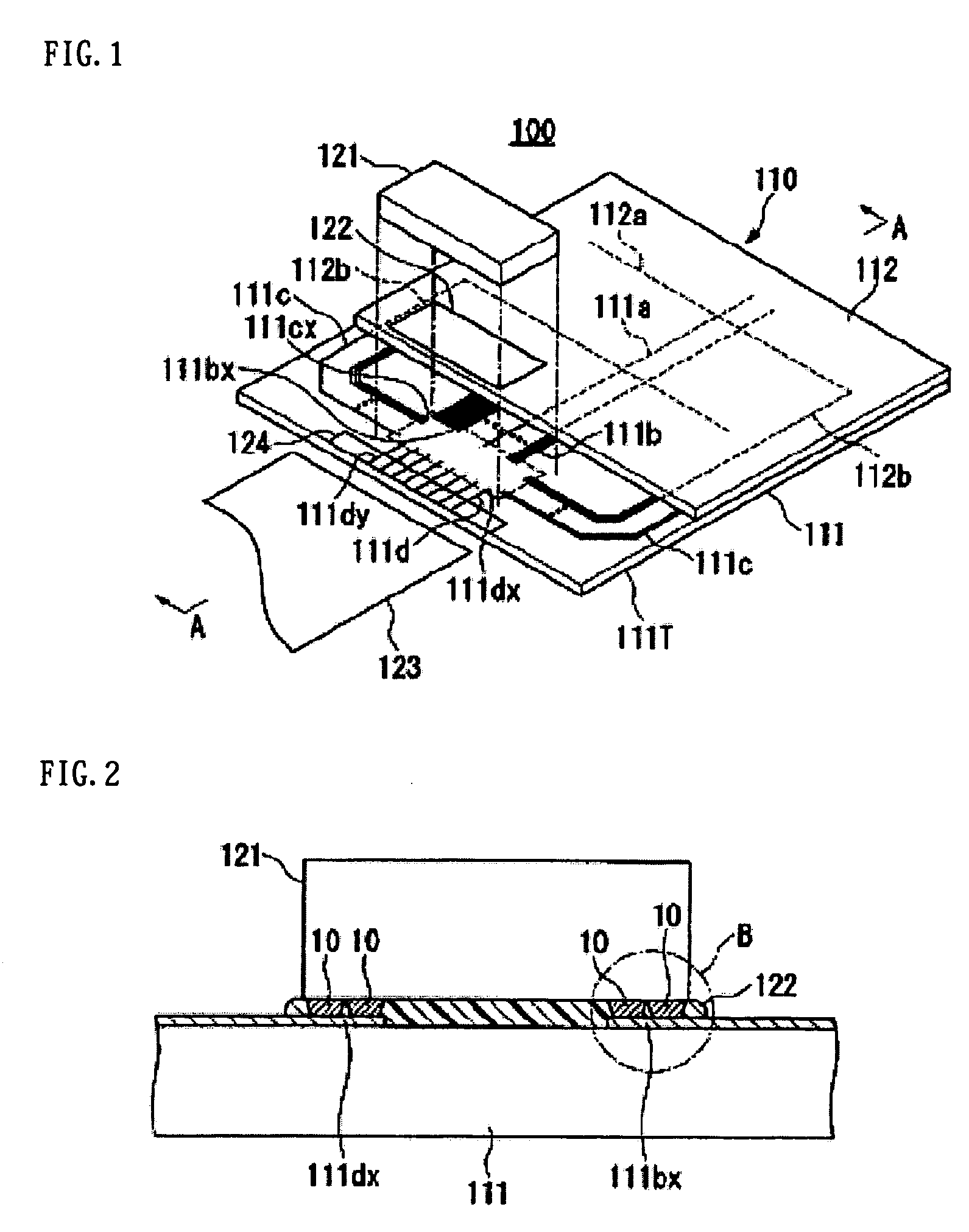
[0046]FIG. 1 is a schematic diagram of a liquid crystal display according to one embodiment of the electro-optical device of the present invention. A liquid crystal display 100 includes a liquid crystal panel 110 and an electronic component (IC chip for driving a liquid crystal) 121. In addition, accessories, such as a polarizer, a reflection sheet, and a backlight, are included as necessary (not shown).

[0047]Electro-optical Device

[0048]The liquid crystal panel 110 includes substrates 111 and 112 made of glass or plastic. The substrate 111 and the substrate 112 are opposed to each other and are laminated with a sealant (not shown). A liquid crystal is contained between the substrate 111 and the substrate 112 as electro-optic material (not shown). An electrode 111a made of a transparent electric conductor, such as indium tin oxide (ITO), is disposed on the inner surface of the substrate 111. An ele...

embodiment 2

[0065

[0066]A second embodiment of the present invention will be described below with reference to FIG. 5.

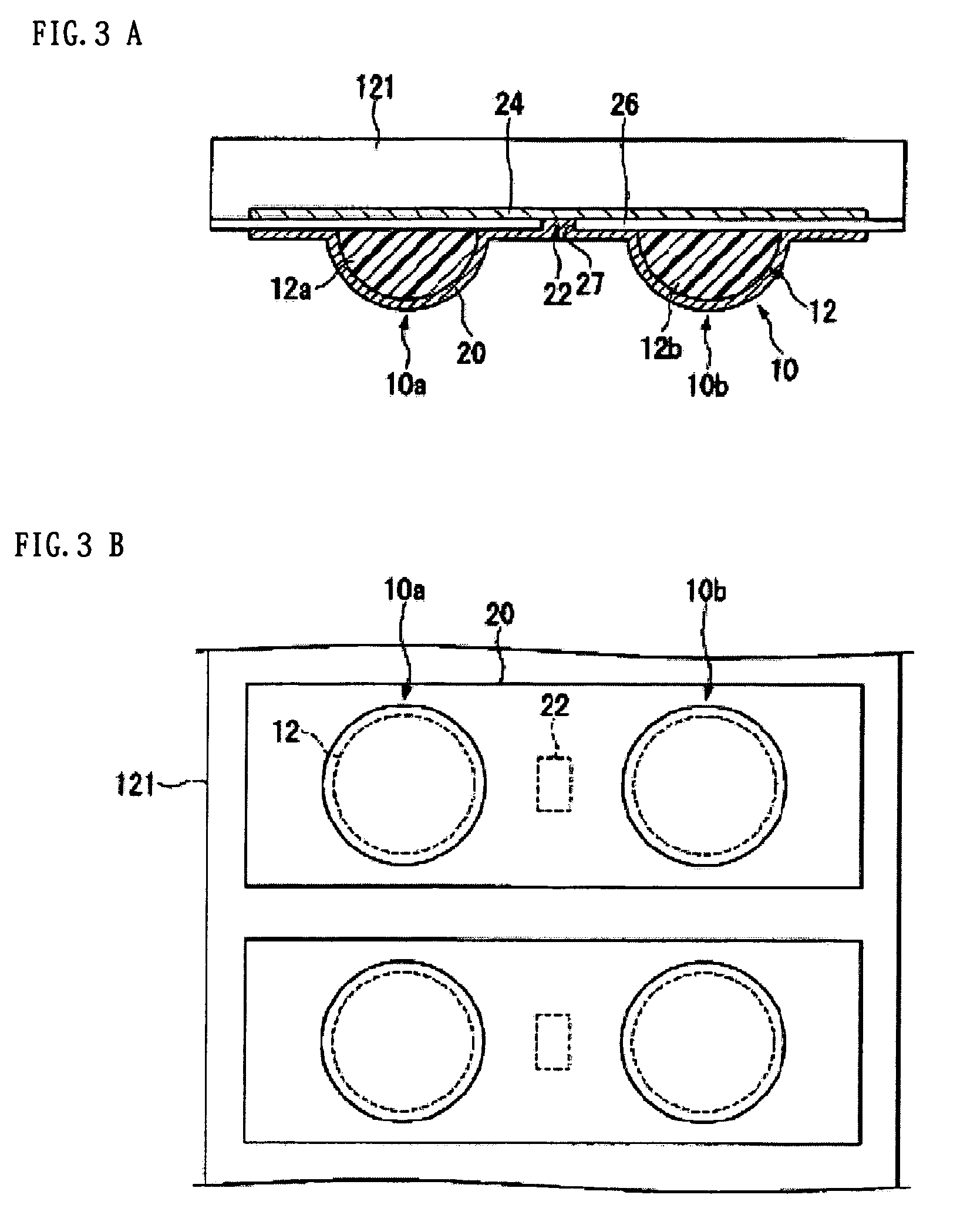
[0067]FIG. 5 is an enlarged view of the portion B in FIG. 2, showing the structure of electrodes in an electronic component according to the second embodiment. The electronic component according to the second embodiment is different from that in the first embodiment in that one bump electrode (for example, 10a) is electrically connected to the pad 24 through a plurality of electrical connectors 22x, 22y, and 22z. Like components are denoted by like numerals in the first embodiment and will not be further explained.

[0068]The electronic component according to the second embodiment has a plurality of openings 27 in the protective coating 26 on the pad 24. These openings function as connectors 22x, 22y, and 22z on the pad 24.

[0069]Hemispherical resin bumps 12 are disposed on the protective coating 26. In FIG. 5, resin bumps 12a and 12b are disposed between the connector 22x and the c...

embodiment 3

[0074

[0075]A third embodiment of the present invention will be described below with reference to FIG. 6.

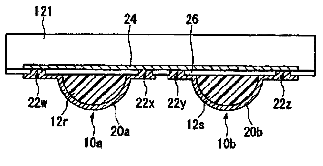
[0076]FIG. 6 shows the structure of electrodes in an electronic component according to the third embodiment. FIG. 6(a) is an enlarged view of the portion B in FIG. 2. FIG. 6(b) is a bottom view of the electronic component. The electronic component according to the third embodiment is different from those in the first and second embodiments in that resin bumps12 (12r and 12s) are formed in linear convex strips and that a plurality of electrically conductive separate films (20a and 20b) are individually connected to the pad 24. Like components are denoted by like numerals in the first and second embodiments and will not be further explained.

[0077]In the electronic component according to the third embodiment, the resin bumps 12r and 12s are formed in linear convex strips in the direction along the pad 24. The transverse cross section of the resin bumps 12r and 12s is semicircular. Su...


PUM


Abstract

An electronic component electrically connected to a counter substrate through a pad on an active surface, characterized in that a resin bump on the active surface and an electrically conductive film on the resin bump constitute a bump electrode, and that a plurality of bump electrodes are electrically connected to the one pad.

Description

RELATED APPLICATIONS[0001]This application claims priority to Japanese Patent Application No. 2004-121645 filed Apr. 16, 2004 which is hereby expressly incorporated by reference herein in its entirety.BACKGROUND[0002]1. Technical Field[0003]The present invention relates to an electronic component, a mounted structure, an electro-optical device, and an electronic device.[0004]2. Related Art[0005]Conventionally, technologies for packaging an electronic component, such as a semiconductor integrated circuit (IC), have been used in circuit boards or liquid crystal displays to be mounted on various electronic devices. For example, an IC chip for driving a liquid crystal panel is mounted on a liquid crystal display. The IC chip may be mounted directly on a glass substrate constituting the liquid crystal panel, or may be mounted on a flexible printed circuit (FPC) to be mounted in the liquid crystal panel. The mounted structure of the former is designated as a chip-on-glass (COG) structure,...

Claims


Application Information

Patent Timeline
Patent Type & Authority Patents(United States)
IPC IPC(8): H01L23/48H01L23/12H01L21/60H01L23/485
CPCH01L24/10H01L24/13H01L2224/13099H01L2924/01013H01L2924/01029H01L2924/01033H01L2924/01049H01L2924/01078H01L2924/01079H01L2924/01082H01L2924/14H01L2924/01005H01L2924/01006H01L2924/01023H01L2924/00H01L2224/05571H01L2224/05573H01L2224/05624H01L2224/13008H01L2224/1319H01L2224/13562H01L2224/1357H01L2224/13644H01L2224/13647H01L2224/13655H01L2224/73204H01L2224/13013H01L24/14H01L24/02H01L24/16H01L2924/0001H01L2224/02379H01L24/05H01L2224/13H01L2924/00014H01L2224/02F24F6/12F24F11/30F24F11/0008F24F3/16F24F2110/20F24F8/22
Inventor SAITO, ATSUSHITANAKA, SHUICHI
Owner BOE TECH GRP CO LTD
Why Eureka
Try Eureka