Multiple data rate interface architecture

a multi-data rate, interface technology, applied in logic circuit coupling/interface arrangement, pulse technique, instruments, etc., can solve the problems of exacerbated constraints, high process voltage and temperature (pvt), and high variability of typical phase shift techniques, so as to facilitate efficient pin migration, facilitate the implementation of larger plds, and be easily scaled in size

Inactive Publication Date: 2007-01-23
ALTERA CORP
View PDF57 Cites 18 Cited by
  • Summary
  • Abstract
  • Description
  • Claims
  • Application Information

AI Technical Summary

Benefits of technology

[0006]The present invention provides method and circuitry for implementing high speed multiple-data-rate interface architectures for programmable logic devices. In one embodiment, the invention employs a delay chain with precise phase shift control to achieve the desired phase shift in the data strobe DQS signal. I/O pins and their corresponding registers are divided into groups, with each group having at least one pin dedicated to the DQS signal and others to data (DQ) signals. An incoming DQS signal goes through the desired phase shift (e.g., 90 degrees) controlled by the phase shift co

Problems solved by technology

However, typical phase shift techniques that use, for example, delay chains, are highly susceptible to process, voltage, and temperature (PVT) variations.
This places further demands on the performance of the phase shift circuitry.
Some of the above constraints, however, are exacerbated when impleme

Method used


Image

  • Multiple data rate interface architecture
  • Multiple data rate interface architecture
  • Multiple data rate interface architecture

Examples


Embodiment Construction

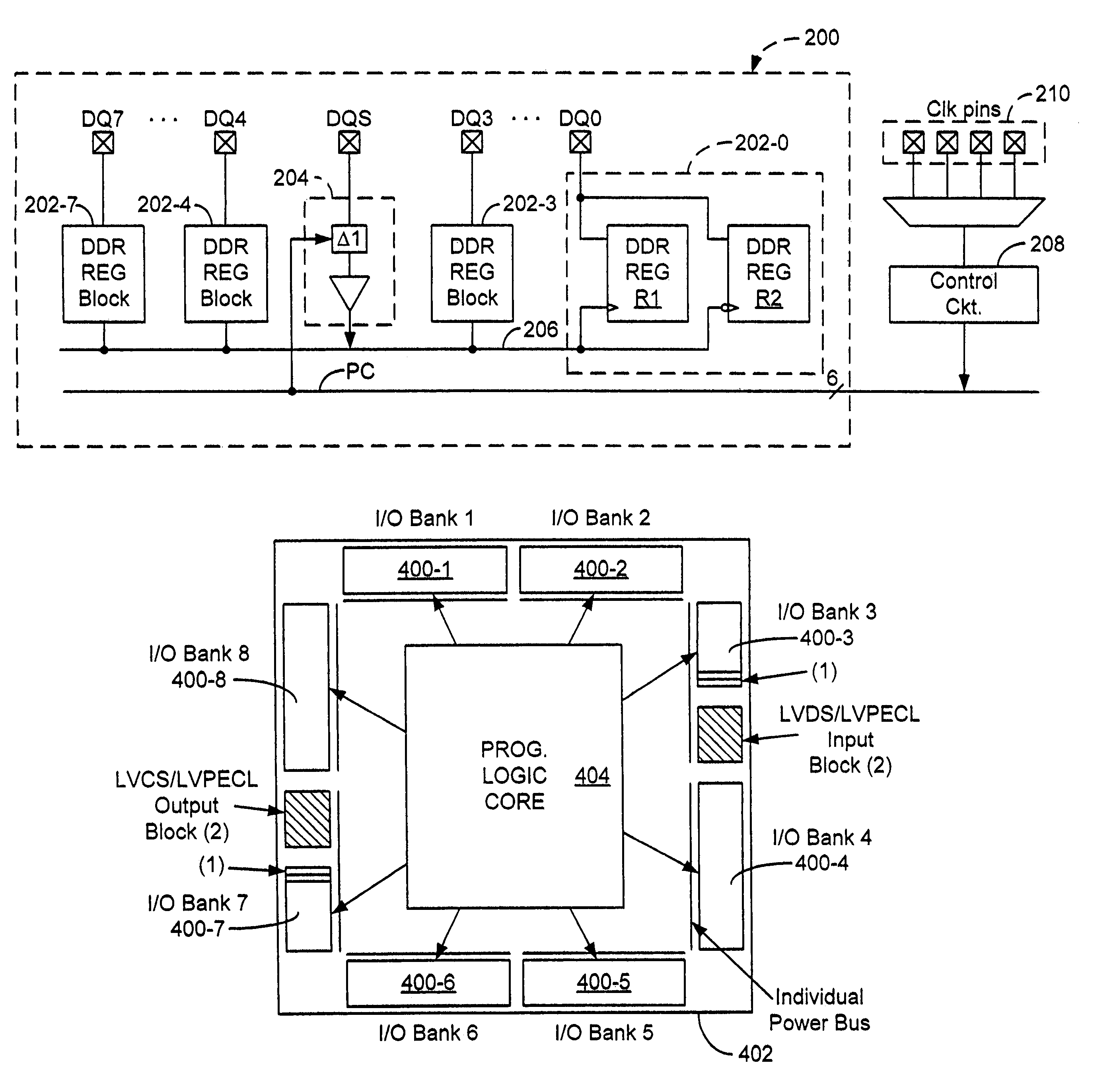
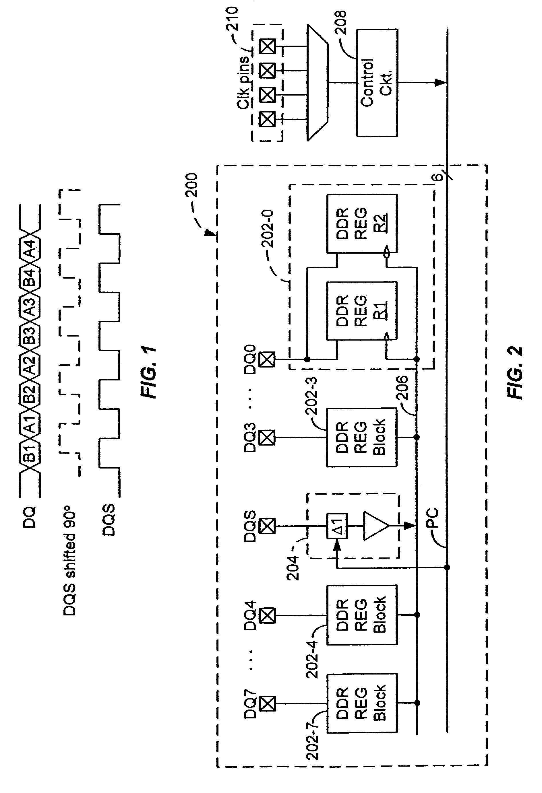
[0018]To minimize skew, accommodate a wide frequency range of operation, and facilitate rapid pin migration to larger PLDs, the present invention provides a modular multiple-data-rate I / O architecture that can be readily replicated and scaled. For illustrative purposes, the invention is described in the context of a double-data rate (DDR) system. It is to be understood, however, that the principles of this invention can be applied to systems operating at quad-data rate or higher. Referring to FIG. 2, there is shown a block diagram of an I / O module 200 for a PLD configured for DDR operation according to one embodiment of the present invention. In this embodiment, DDR interface module 200 includes a number of, in this example eight, data I / O cells each having a data I / O pin DQ and a DDR register block 202 made up of a pair of data registers R1 and R2. Module 200 also includes a strobe input cell which is preferably located at a central location vis à vis other I / O cells, and includes ...


PUM


Abstract

Method and circuitry for implementing high speed multiple-data-rate interface architectures for programmable logic devices. The invention partitions I/O pins and their corresponding registers into independent multiple-data rate I/O modules each having at least one pin dedicated to the strobe signal DQS and others to DQ data signals. The modular architecture facilitates pin migration from one generation of PLDs to the next larger generation.

Description

CROSS-REFERENCES TO RELATED APPLICATIONS[0001]This application is related to commonly-assigned, co-pending U.S. patent application Ser. No. 10 / 037,861, filed Jan. 2, 2002 entitled “Self-Compensating Delay Chain for Multiple Data-Rate Interfaces,” by Chong et al., which is hereby incorporated by reference in its entirety.BACKGROUND OF THE INVENTION[0002]The present invention relates in general to input / output (I / O) interface in integrated circuits, and in particular to method and circuitry for distributing clock signals in a programmable logic device (PLD) that employs a multiple data rate interface.[0003]To address the data bandwidth bottleneck in the interface between integrated circuits, high speed interface mechanisms have been developed which have helped increase the speed of data transfer and data throughput. In a multiple data rate interface scheme, two or more bits of data are transferred during each clock period. One example of multiple data rate is the so called double data...

Claims


Application Information

Patent Timeline
IPC IPC(8): H01L25/00H03K19/177
CPCH03K19/017581H03K19/17744
Inventor PAN, PHILIPSUNG, CHIAKANGHUANG, JOSEPHCHONG, YANWANG, BONNIE I.
Owner ALTERA CORP
Why Eureka
Try Eureka