Dual-band CMOS front-end with two gain modes

a cmos front-end and gain mode technology, applied in the direction of gated amplifiers, low-noise amplifiers, transportation and packaging, etc., can solve the problems of increasing the number of chip components, the overall die size, and the die cost is significantly increased, so as to improve the effect of reducing the footprint of the rf receiver

Inactive Publication Date: 2007-01-23
O KENNETH K +1
View PDF9 Cites 47 Cited by
  • Summary
  • Abstract
  • Description
  • Claims
  • Application Information

AI Technical Summary

Problems solved by technology

This conventional arrangement increases the number of chip components and thus the overall die size, which in turn significantly increases the die cost.

Method used


Image

  • Dual-band CMOS front-end with two gain modes
  • Dual-band CMOS front-end with two gain modes
  • Dual-band CMOS front-end with two gain modes

Examples


examples

[0044]The present invention is further illustrated by the following specific examples, which should not be constructed as limiting the scope or content of the invention in any way.

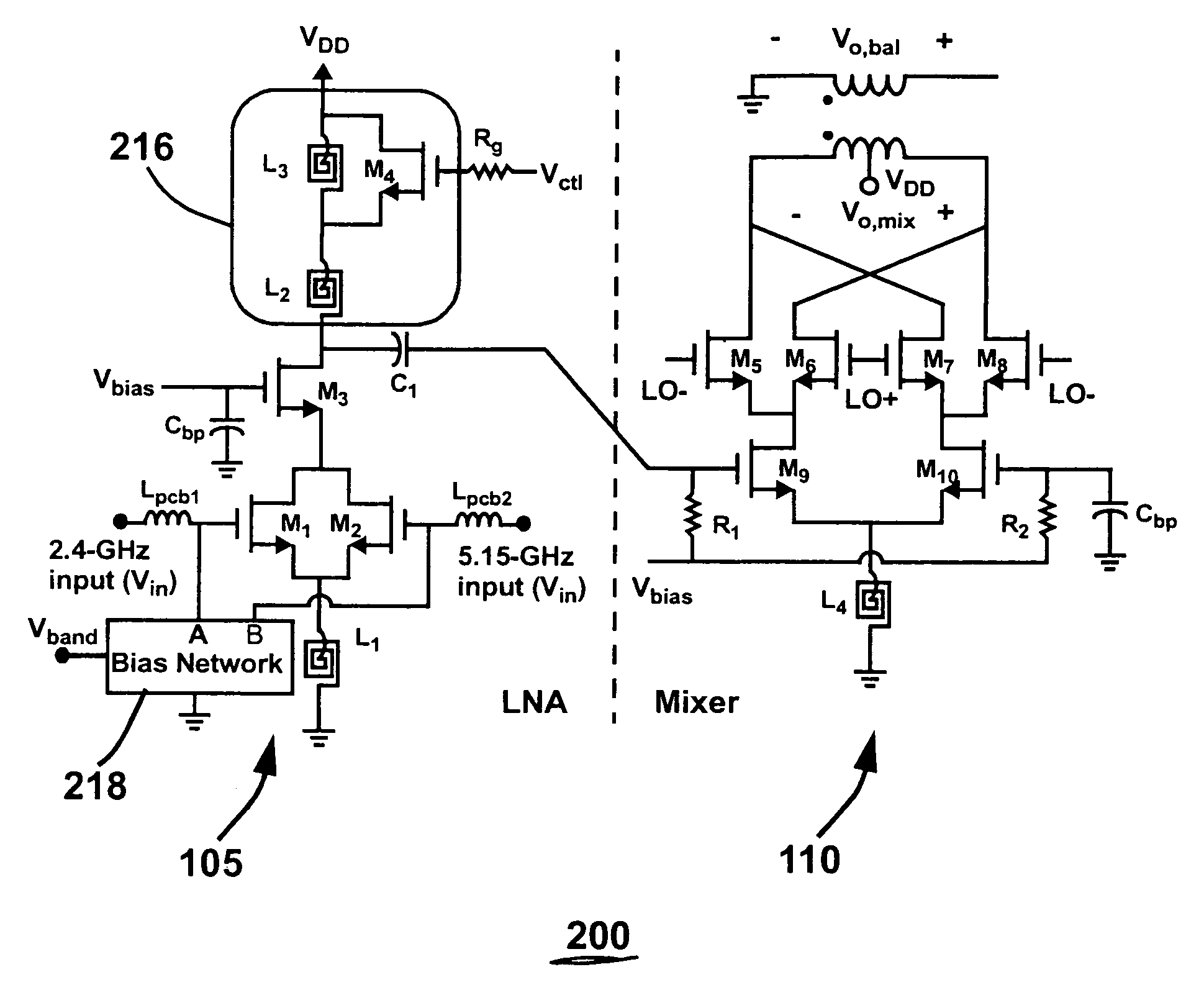
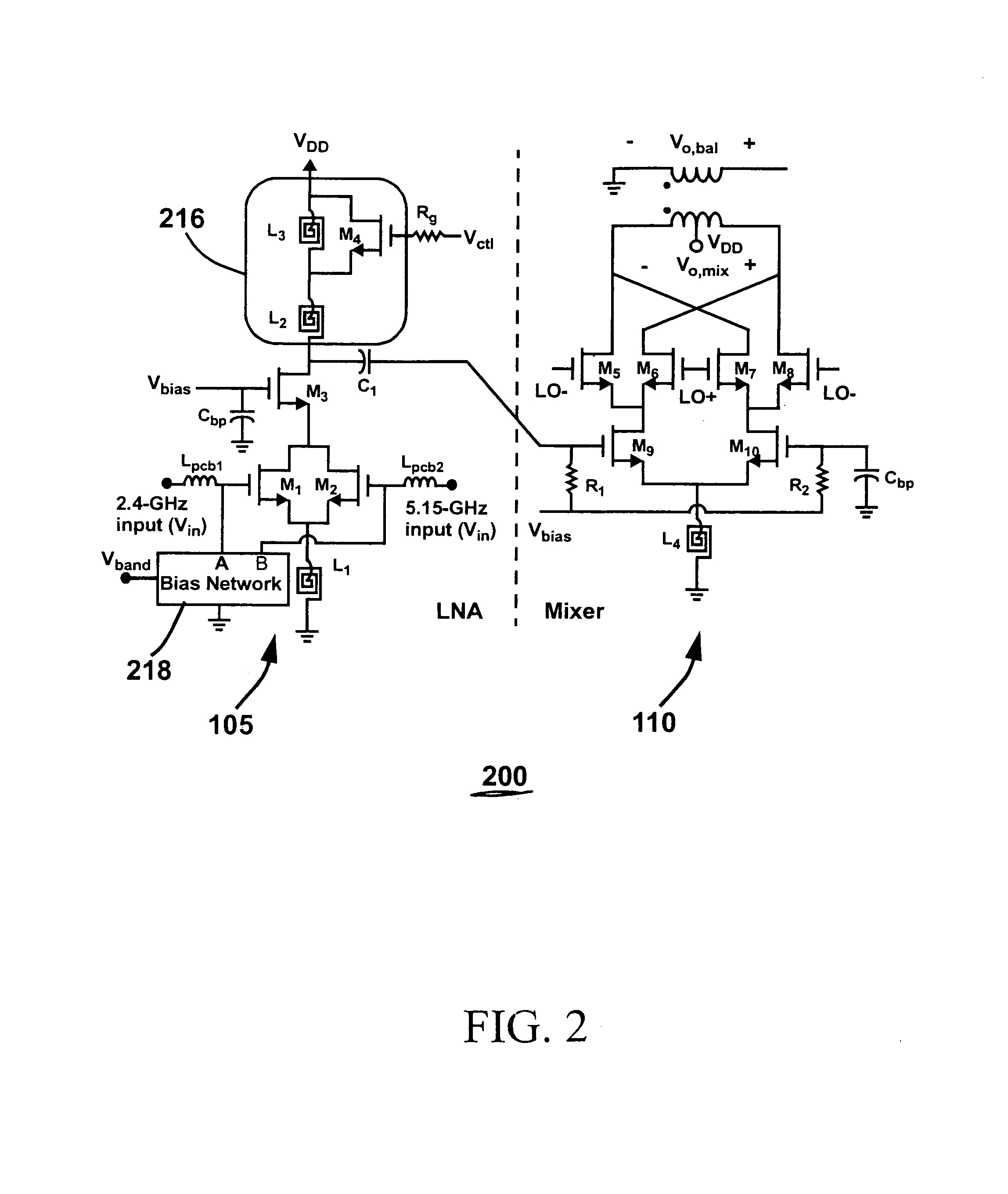
[0045]The RF front-end circuit mounted on a four-layer FR4 board shown in FIG. 6 was tested. Chip-On-Board (COB) packaging technique was used for the testing, where a fabricated bare die according to the invention was directly bonded to the Printed-Circuit Board (PCB). The measured dual-band front-end circuit characteristics are summarized in Table 2 below.

[0046]

TABLE 2Frequency(GHz)2.45.15Gain Control ModeHighLowHighLowPower Gain (dB)26.59.51710Voltage Gain (dB)39.822.829.222.2DSB NF (dB)1.54.1SSB NF Calculated from2.66.2DSB NF (dB) [15]Input P1dB (dBm)−21−17−12−9.5P1dB (dBm)4.5−8.54−0.5Input IP3 (dBm)−12.7−6.6−4.1−1IP3 (dBm)13.82.912.99S11(dB)−8−8−10.8−10.8LO to IF Isolation (dB)>30>25VDD(V)1.81.81.81.8LNA Current (mA)339.19.1Mixer Current (mA)10.610.61414

[0047]A 2.4-GHz band power gain versus frequency ...


PUM


Abstract

A multi-band low noise amplifier (LNA) 105 includes an input stage having at least two inputs, a first input (103) coupled to a first input transistor for receiving signals in a first frequency band and a second input (104) coupled to a second input transistor for receiving signals in a second frequency band. The second frequency band spaced apart from the first frequency band. A bias network (218) having a band select input is coupled to the first and second input transistor, wherein a signal level applied to the band select input turns on one of the input transistors and turns off the other input transistors. The LNA (105) operates in the first frequency band when the first input transistor is on and the second frequency band when the second input transistor is on. A switched resonator (216) having a control input is provided, wherein application of a control signal to the control input tunes a resonant frequency of the LNA, and provides gain select, for operation in either the first or second frequency band.

Description

CROSS-REFERENCE TO RELATED APPLICATIONS[0001]This application claims the benefit of U.S. Provisional Application No. 60 / 569,744 Entitled DUAL-BAND CMOS FRONT-END WITH TWO GAIN MODES filed on May 10, 2004, the entirety of which is incorporated herein by reference.STATEMENT REGARDING FEDERALLY SPONSORED RESEARCH OR DEVELOPMENT[0002]Not applicable.FIELD OF THE INVENTION[0003]The invention relates to receive circuitry for multi-band operation using a single set of tunable RF blocks with gain control.BACKGROUND OF THE INVENTION[0004]As wireless applications proliferate, the demands for radios which can support multiple bands and multiple standards are rapidly increasing. These demands are typically addressed by having two or three sets of band separated RF blocks to handle the separate bands, as well as a baseband blocks to support each RF block. This conventional arrangement increases the number of chip components and thus the overall die size, which in turn significantly increases the ...

Claims


Application Information

Patent Timeline
Patent Type & Authority Patents(United States)
IPC IPC(8): H03G3/20H03F1/02H03F1/42H03F3/191H03F3/45H03F3/72H03G1/00
CPCH03F1/0261H03F1/42H03F3/191H03F3/45188H03G1/0088H03F3/72H03F2200/111H03F2200/294H03F2200/372
Inventor LI, ZHENBIAOO, KENNETH K
Owner O KENNETH K
Why Eureka
Try Eureka