Unlock instant, AI-driven research and patent intelligence for your innovation.

Apparatus and method for programming a memory array

a memory array and programming method technology, applied in the field of methods and apparatus for programming a memory array, can solve the problems of inability to implement current charge storage approaches, and achieve the effect of avoiding current charges

Inactive Publication Date: 2007-01-23
INTEL CORP
View PDF6 Cites 50 Cited by
  • Summary
  • Abstract
  • Description
  • Claims
  • Application Information

AI Technical Summary

Benefits of technology

The invention relates to a method and apparatus for programming a memory array with one-time programmable (OTP) cells. The OTP cells are programmed using a combination of charge storage and fuse elements. The charge storage approach uses a thin oxide layer to break down the oxide layer and set the value of the cell based on the charge stored in the insulated MOS transistor. The fuse elements are programmed by applying a high voltage to the oxide layer, which causes a short circuit. The invention is particularly useful for deep sub-micron technologies where the oxide layer is thinner and the leakage current is higher. The invention also includes a memory array with OTP cells and an apparatus for programming it.

Problems solved by technology

Such charge storage approaches, however, are not practicable with current and future deep sub-micron technologies that feature very thin gate oxide because of the high gate leakage current that prevents a long retention time of the information.

Method used


Image

  • Apparatus and method for programming a memory array
  • Apparatus and method for programming a memory array
  • Apparatus and method for programming a memory array

Examples


Embodiment Construction

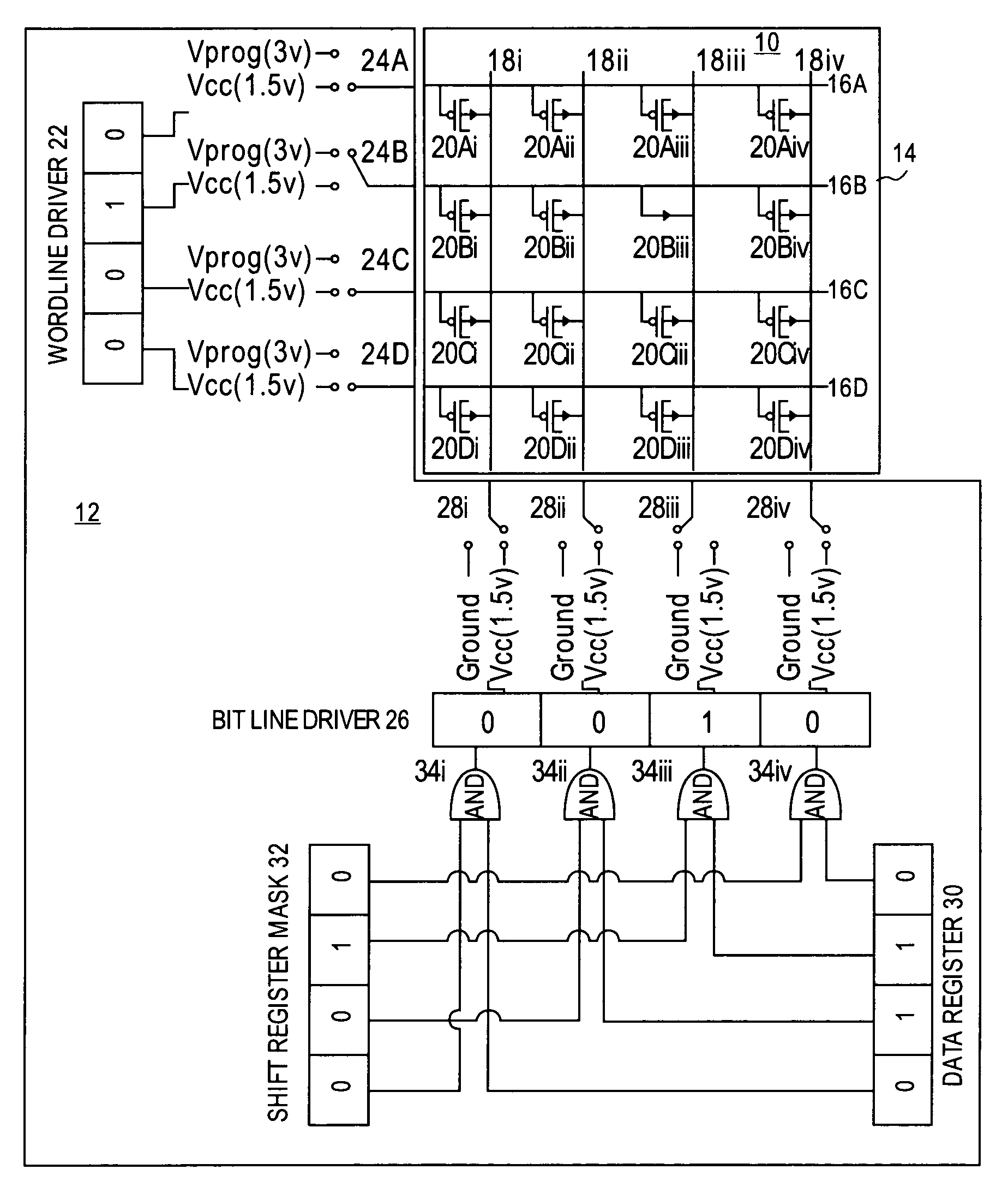
[0018]FIG. 1 of the accompanying drawings illustrates a memory array 10 and an apparatus 12 that is used to program the memory array 10, according to an embodiment of the invention.

[0019]The memory array 10 has a semiconductor substrate 14 and a plurality of components formed in and on the substrate 14, including a plurality of word lines 16, a plurality of bit lines 18, and a plurality of bits 20. The word lines 16 extend in an x-direction, and the bit lines 18 extend in a y-direction across the substrate 14. Each bit 20 is connected between one of the word lines 16 and one of the bit lines 18 near an intersection of the respective word line 16 and bit line 18. The bits 20 thus form an x-y array across the substrate 14.

[0020]The bits 20 are initially PMOS transistors with a gate of the PMOS transistor to connect it to the word line 16, and both the source and the drain of the PMOS transistor connected to a bit line18. A voltage of at least three volts applied to the gate of the PMO...


PUM


Abstract

A method of programming a memory array is provided, including accessing a plurality of word lines of the memory array by providing a plurality of voltage steps sequentially after one another to the respective word lines, and accessing a plurality of bit lines of the memory array each time that a respective word line is accessed, to program a plurality of devices corresponding to individual word and bit lines that are simultaneously accessed, each device being programmed by breaking a dielectric layer of the device, accessing of the bit lines being sequenced such that only a single one of the devices is programmed at a time.

Description

BACKGROUND OF THE INVENTION[0001]1). Field of the Invention[0002]Embodiments of this invention relate to a method and apparatus for programming a memory array.[0003]2). Discussion of Related Art[0004]One-time programmable (“OTP”) cells are used in integrated circuit (“IC”) devices for a variety of applications including OTP memory applications. They may be used as a single memory cell or in arrays of memory cells to provide unique die / chip IDs and to set operating parameters such as clock multipliers and voltage levels for devices such as microprocessors. They may also be used to configure, customize, and repair a chip after testing (e.g., to repair a processor chip's cache memory array). OTP cells are typically implemented using charge storage, fuse, or anti-fuse approaches. Charge storage approaches have typically involved defining a bit value based on charge stored on an insulated metal oxide semiconductor (“MOS”) type gate structure. Such charge storage approaches, however, are ...

Claims


Application Information

Patent Timeline
Patent Type & Authority Patents(United States)
IPC IPC(8): G11C16/04
CPCG11C17/18
Inventor PAILLET, FABRICEKESHAVARZI, ALIKHELLAH, MUHAMMAD M.SOMASEKHAR, DINESHYE, YIBINTANG, STEPHEN H.ALAVI, MOHSENDE, VIVEK K.KARNIK, TANAY
Owner INTEL CORP