

Oversampling clock recovery circuit applicable not only to high rate data but also to low rate data
a recovery circuit and high rate data technology, applied in logic circuits, multi-function communication, digital transmission, etc., can solve the problems of difficult implementation of inability to use the oversampling clock recovery circuit for 2.5 gbps data rate, and inability to implement delay buffer operable at a very little propagation delay
- Summary
- Abstract
- Description
- Claims
- Application Information
AI Technical Summary
Benefits of technology
Problems solved by technology
Method used
Image

Examples
first embodiment
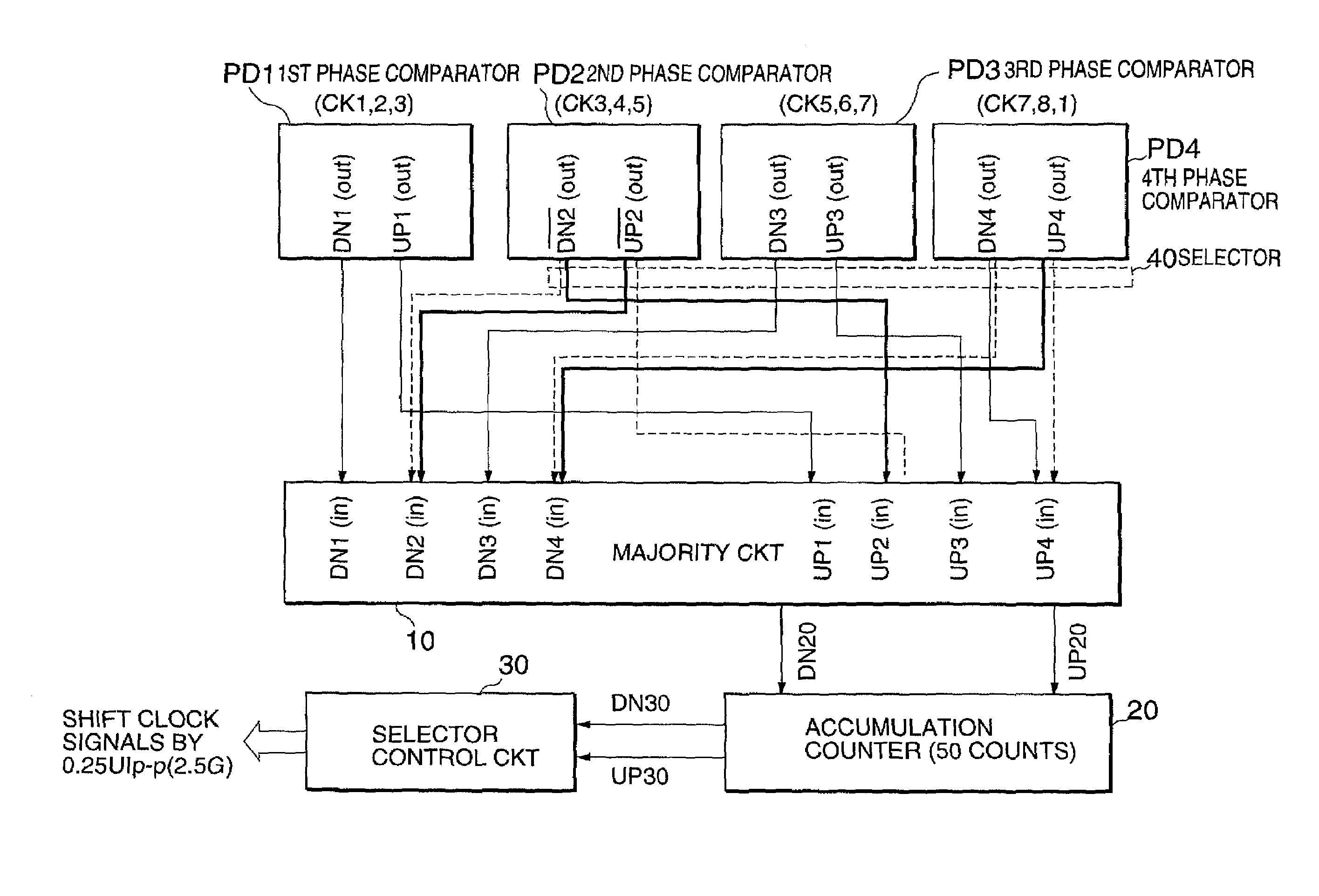
[0120]Referring to FIGS. 5A through 5F and FIG. 6, the description will proceed to an oversampling clock recovery circuit according to a first embodiment of this invention. FIG. 5A is a time chart schematically showing a waveform of an input data DT2. FIGS. 5B through 3D are time charts schematically showing leading edges of eight-phase clock signals CK1 through CK8. FIGS. 5E and 5F show a phase comparison characteristic in phase comparators. FIG. 6 is a block diagram showing a main part of the digital oversampling clock recovery circuit that includes the phase comparators.
[0121]As shown in FIG. 5A, the input data DT2 is a serial input data having a data rate of 1.25 Gbps and has a length of one bit equal to 800 ps. Flicker in the input data DT2 caused by jitter is dependent on the data rate. Inasmuch as it is convenient to use, as an indicator of a magnitude of the flicker, a unit of a bit length, a length of one bit is represented by 1UI (unit interval) in the art. Inasmuch as the...
second embodiment
[0144]Referring to FIGS. 7A through 7F and FIG. 8, the description will proceed to a 2-times digital oversampling clock recovery circuit according to a second embodiment of this invention. FIG. 7A is a time chart schematically showing a waveform of an input data DT3. FIGS. 7B through 7D are time charts schematically showing leading edges of eight-phase clock signals CK1 through CK8. FIGS. 7E and 7F show a phase comparison characteristic in phase comparators. FIG. 8 is a block diagram showing a main part of the 2-times digital oversampling clock recovery circuit that includes the phase comparators.
[0145]As shown in FIG. 7A, the input data DT3 is a serial input data having a data rate of 622 Mbps and has a length of one bit equal to 1600 ps. Flicker in the input data DT3 caused by jitter is dependent on the data rate. Inasmuch as it is convenient to use, as an indicator of a magnitude of the flicker, a unit of a bit length, a length of one bit is represented by 1 UI (unit interval) in...
third embodiment
[0191]Referring to FIGS. 11A through 11F and FIG. 12, the description will proceed to an oversampling clock recovery circuit according to a third embodiment of this invention. FIG. 11A is a time chart schematically showing a waveform of an input data DT2. FIGS. 11B through 11D are time charts schematically showing leading edges of sixteen-phase clock signals CK1 to CK8 and CK1D to CK8D. FIGS. 11E and 11F show a phase comparison characteristic in phase comparators. FIG. 12 is a block diagram showing a main part of the digital oversampling clock recovery circuit that includes the phase comparators.
[0192]As shown in FIG. 11A, the input data DT2 is a serial input data having a data rate of 1.25 Gbps and has a length of one bit equal to 800 ps. Flicker in the input data DT2 caused by jitter is dependent on the data rate. Inasmuch as it is convenient to use, as an indicator of a magnitude of the flicker, a unit of a bit length, a length of one bit is represented by 1UI (unit interval) in ...
PUM
 Abstract
Description
Claims
Application Information