Material architecture for the fabrication of low temperature transistor

a technology of low temperature transistors and materials, applied in the direction of transistors, electric devices, solid-state devices, etc., to achieve the effect of reducing repetition

Active Publication Date: 2007-01-30
CHARTERED SEMICONDUCTOR MANUFACTURING
View PDF8 Cites 164 Cited by
  • Summary
  • Abstract
  • Description
  • Claims
  • Application Information

AI Technical Summary

Problems solved by technology

However, during the anneal, damage from the ion implantation process, in the form of point defects, migrates laterally from the source and / or drain and into the semiconductor body and enhances dopant diffusion.
An additional challenge is the development of processing-compatible methods of controlling the diffusion of dopant atoms.

Method used


Image

  • Material architecture for the fabrication of low temperature transistor
  • Material architecture for the fabrication of low temperature transistor
  • Material architecture for the fabrication of low temperature transistor

Examples


example embodiment

III. OVERVIEW—GENERAL EXAMPLE EMBODIMENT

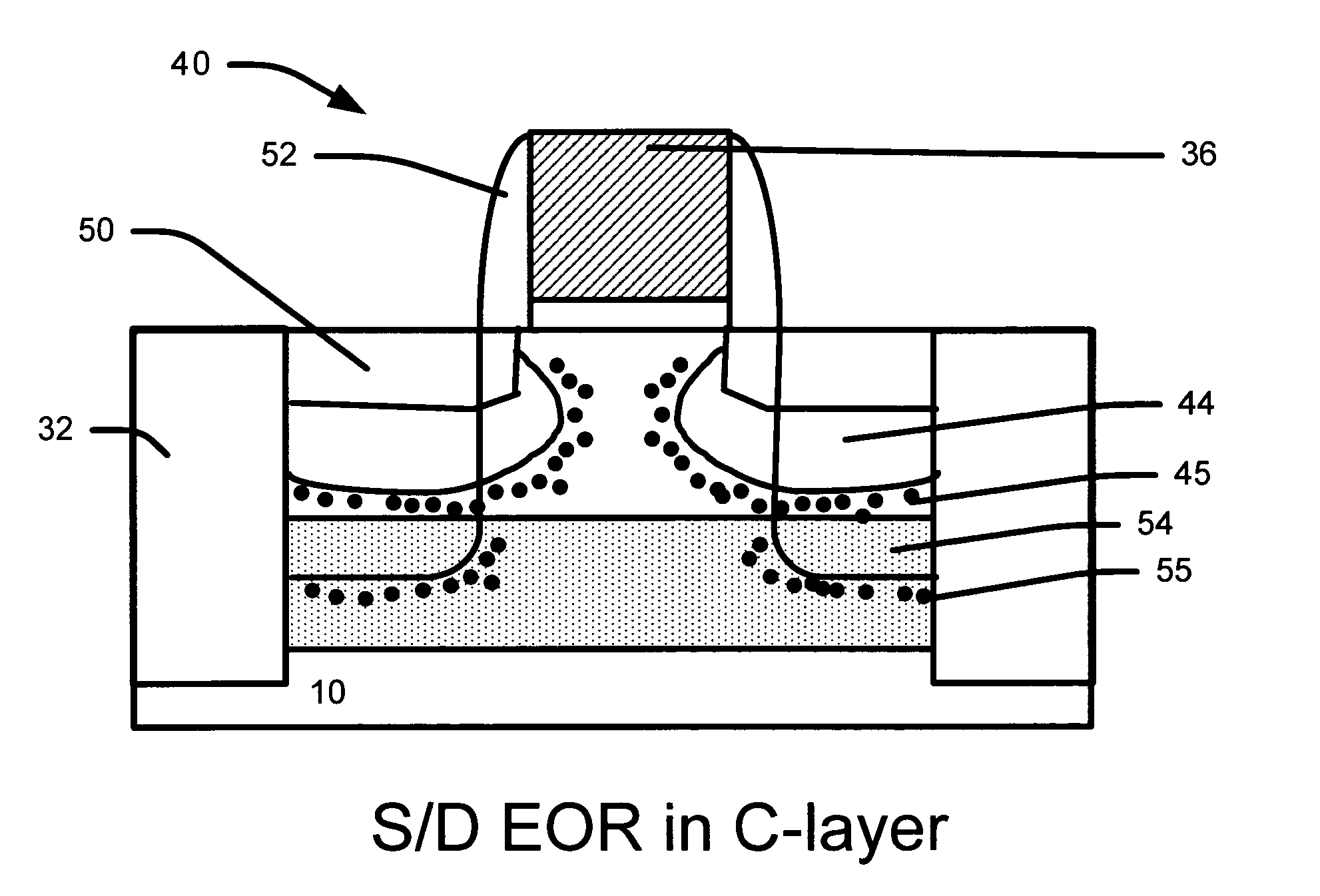
[0073]Some example embodiments form a carbon-containing layer in the EOR regions of an implanted (e.g.,) doped region in a silicon containing substrate. The carbon-containing layer and the implanted region can be formed in any order. The carbon-containing layer helps reduce defects from the implant that formed the implanted or doped region.

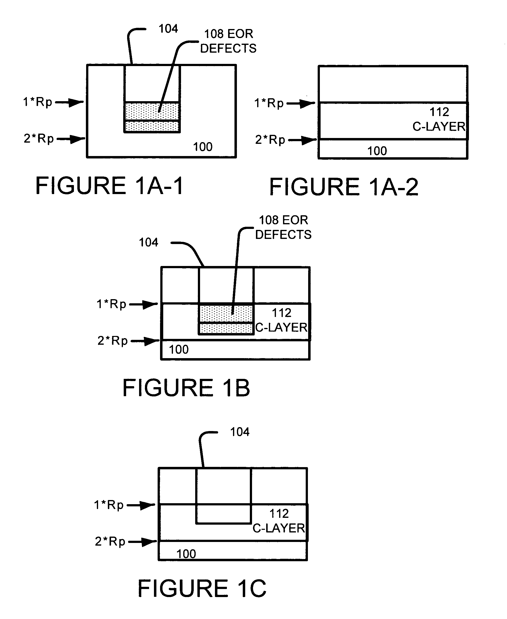
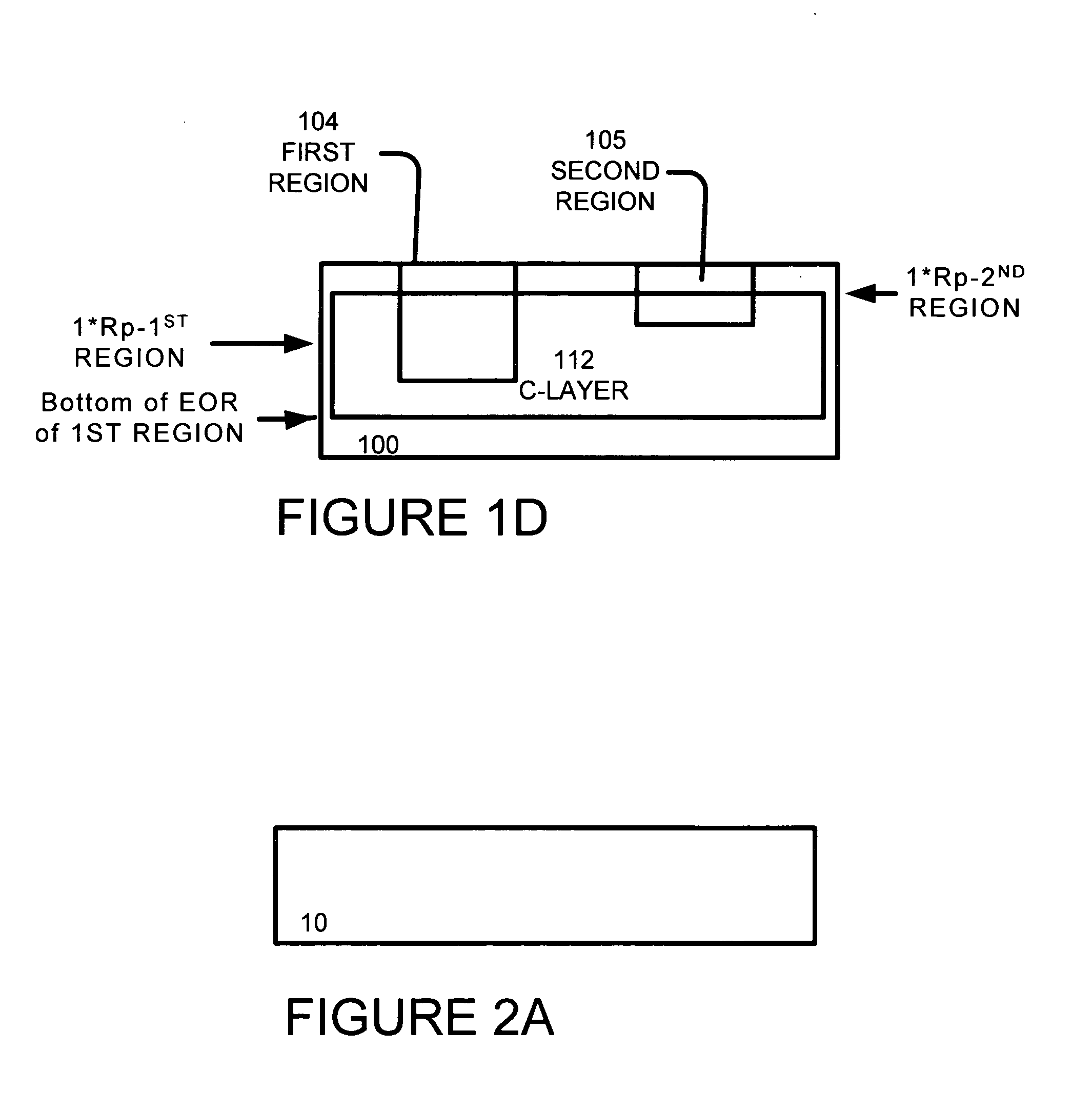
[0074]FIGS. 1A-1 and 1A-2 show the formation of the doped (can be active or non-active ion) or implanted region 104 and the carbon-containing layer 112. These steps may be formed in any order.

[0075]Referring to FIG. 1A-1, a region 104 is formed by an implant process. FIG. 1A-1 shows the depth of the projected range (Rp) or (1*Rp) of the implant and 2 times the depth of the projected range (2*Rp).

[0076]FIG. 1A-2 shows a carbon-containing layer 112 in a substrate. The carbon-containing layer 112 is preferably formed at in at least the EOR region of the implanted region. The EOR region is estimated to be at abo...


PUM

PropertyMeasurementUnit
timeaaaaaaaaaa
timeaaaaaaaaaa
thicknessaaaaaaaaaa

Abstract

A structure and method for forming a carbon-containing layer in at least a portion of the end of range regions of implanted PAI and / or doped regions. The C-containing layer / region getters defects from the implanted PAI region or doped region. Example embodiments show a C-containing layer under at FET. Other example embodiments show an implanted C-containing regions implanted into the EOR region of implanted doped regions, such as pocket regions, S / D regions and SDE regions. Low temperature anneals can be used because the carbon-containing layer reduces defects.

Description

BACKGROUND OF INVENTION [0001]1) Field of the Invention[0002]This invention relates generally to the structure and fabrication of a semiconductor device and more particularly to the fabrication of a carbon containing layer near doped regions in a transistor.[0003]2) Description of the Prior Art[0004]Semiconductor devices such as field effect transistors (FETs) have a source region, and a drain region formed in a semiconductor substrate and a gate formed over the channel region. The source and drain are formed in a semiconductor substrate by introducing impurities (dopants) into the substrate. The semiconductor body separates the source region and the drain region. The dopants used to form the source and drain regions are of a different polarity (n-type or p-type) than the semiconductor substrate body surrounding the source and drain regions. Consequently, substantially no current will pass from the source to the semiconductor body or from the drain to the semiconductor body.[0005]Th...

Claims


Application Information

Patent Timeline
Patent Type & Authority Patents(United States)
IPC IPC(8): H01L21/336
CPCH01L21/26506H01L21/26513H01L29/6659H01L29/1054H01L21/823807H01L29/1083H01L21/823814H01L21/2658
Inventor TAN, CHUNG FOONGLIU, JINPINGLEE, HYEOKJAETEE, KHENG CHOKQUEK, ELGIN
Owner CHARTERED SEMICONDUCTOR MANUFACTURING
Why Eureka
Try Eureka