Circuit and method for testing embedded DRAM circuits through direct access mode

a technology of direct access and circuit, applied in the direction of electronic circuit testing, static storage, measurement devices, etc., can solve the problems of no possibility to collect fail bits, complex redundancy calculation methods, and inability to collect fail bits

Inactive Publication Date: 2007-01-30
POLARIS INNOVATIONS LTD
View PDF9 Cites 38 Cited by
  • Summary
  • Abstract
  • Description
  • Claims
  • Application Information

AI Technical Summary

Benefits of technology

[0011]The present invention provides a circuit and method for testing an eDRAM through a test controller with direct access (DA) mode logic. The circuit and method of the present invention allows the testing of eDRAMs with a conventional memory tester.

Problems solved by technology

However, the test controller with BIST functionality has one major drawback.
There is no possibility to collect a fail bit map and to build in complex redundancy calculation methods for enhanced repairability of the ASIC.

Method used


Image

  • Circuit and method for testing embedded DRAM circuits through direct access mode
  • Circuit and method for testing embedded DRAM circuits through direct access mode
  • Circuit and method for testing embedded DRAM circuits through direct access mode

Examples


Embodiment Construction

[0031]Preferred embodiments of the present invention will be described herein below with reference to the accompanying drawings. In the following description, well-known functions or constructions are not described in detail since they would obscure the invention in unnecessary detail.

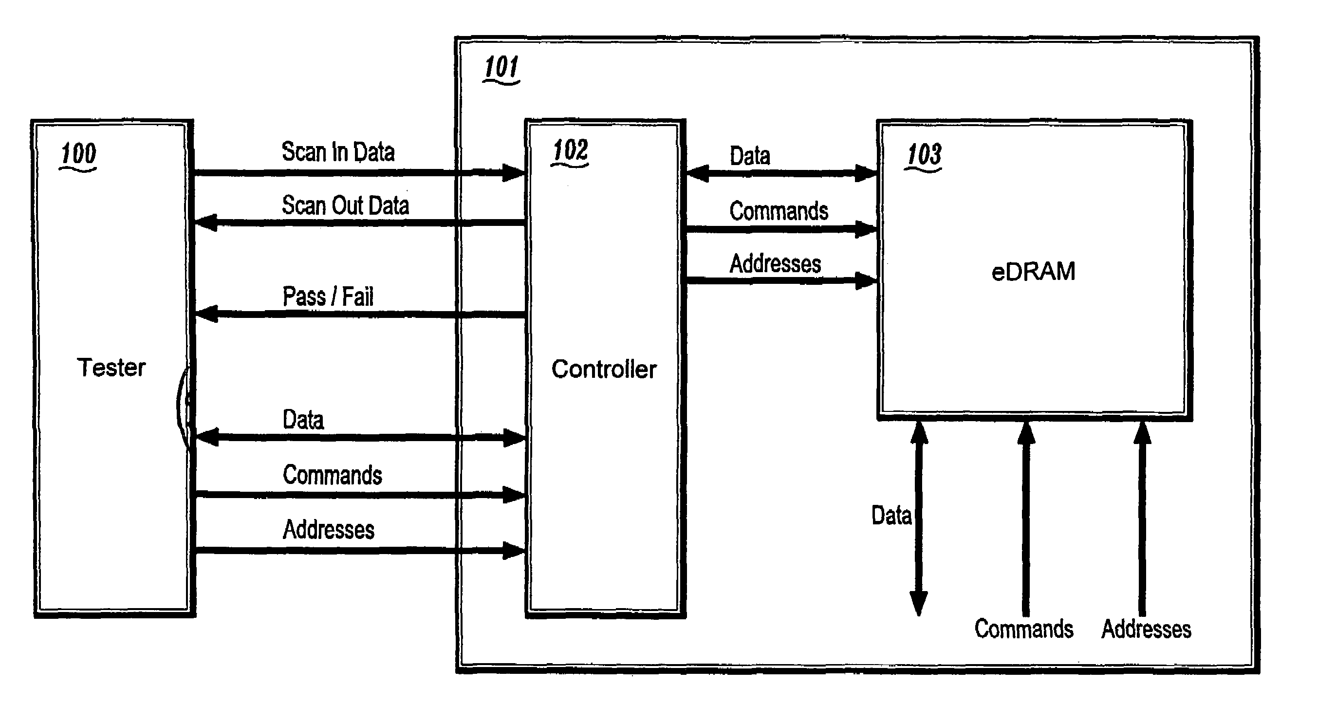
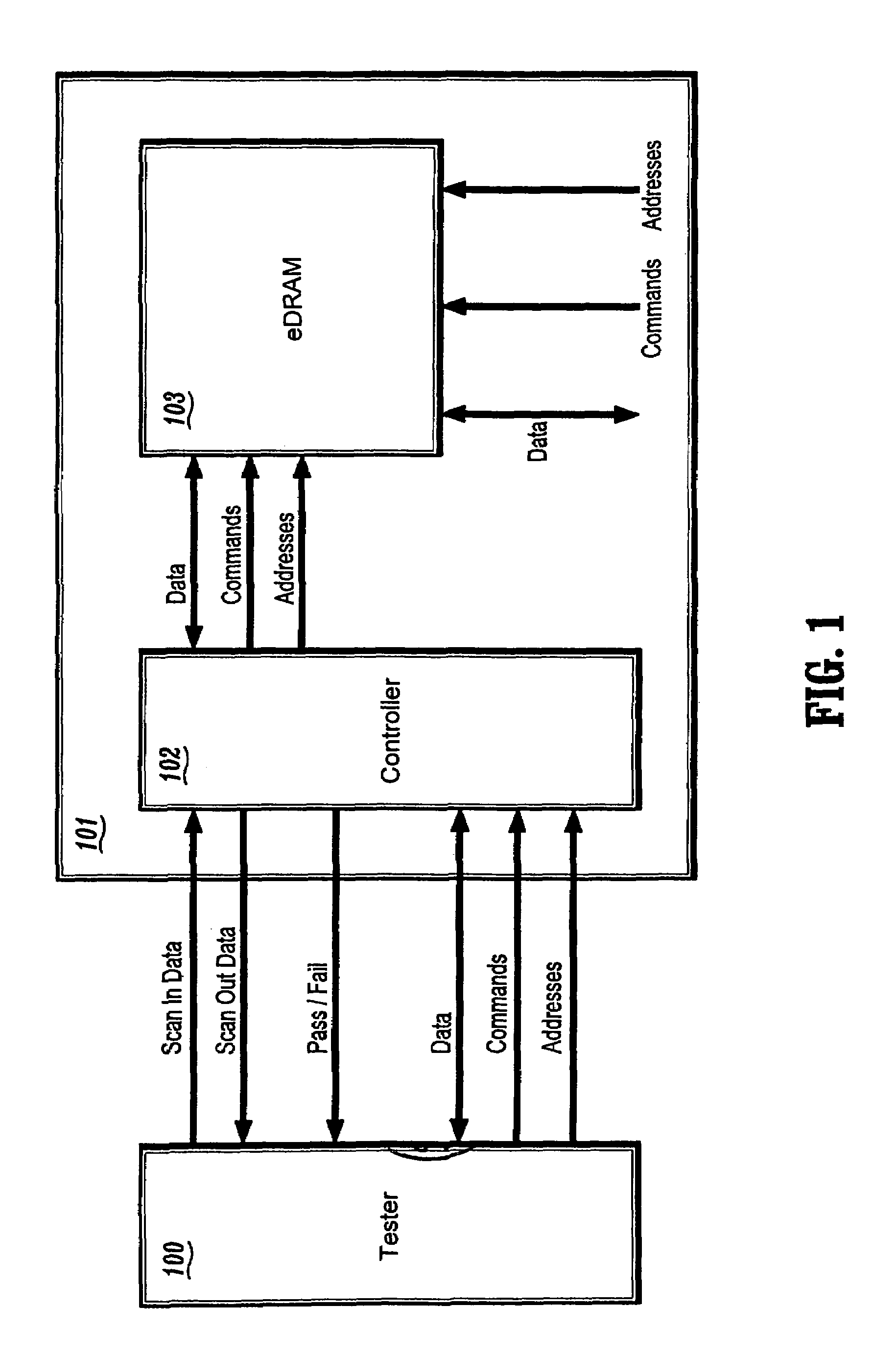
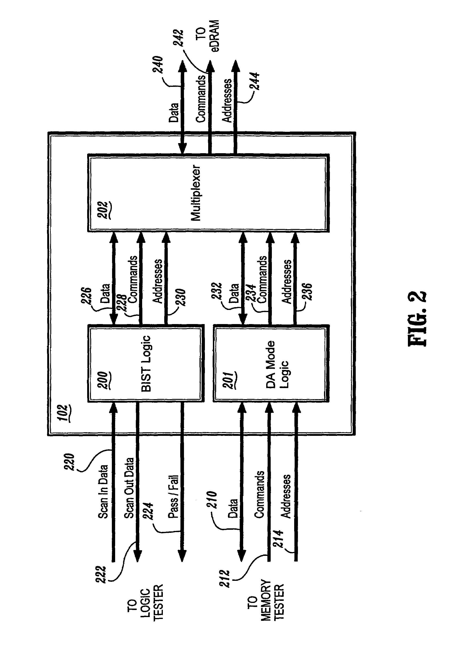
[0032]The present invention provides a circuit and method for testing an embedded DRAM (eDRAM) circuit through a test controller with Direct Access mode (DA mode) logic. FIG. 1 is a block diagram of a test system including a memory device, e.g. an eDRAM, having a test controller with Direct Access mode logic in accordance with the present invention. Referring to FIG. 1, a memory or logic tester 100 is coupled to an ASIC (Application Specific Integrated Circuit) 101 including a test controller 102 and at least one embedded DRAM (eDRAM) 103. The eDRAM 103 includes a plurality of wordlines intersected by a plurality of bitlines having memory cells arranged at respective intersections of the wordlines and ...


PUM


Abstract

A circuit and method for testing an eDRAM through a test controller with direct access (DA) mode logic is provided. The circuit and method of the present invention allows the testing of eDRAMs with a conventional memory tester. The present invention provides a semiconductor device including an embedded dynamic random access memory (eDRAM) for storing data, the eDram including a plurality of memory cells, and a test controller for testing the plurality of memory cells to determine if the cells are defective, the test controller including built-in self-test (BIST) logic circuitry for performing tests and for interfacing to a logic tester, and direct access mode logic circuitry for interfacing the eDRAM with an external memory tester. The test controller further comprises a multiplexer for multiplexing data, commands, and addresses from the BIST logic circuitry and the direct access mode logic circuitry to the eDRAM.

Description

BACKGROUND OF THE INVENTION[0001]1. Field of the Invention[0002]The present invention relates generally to semiconductor device design, and more particularly, to a circuit and method for testing an embedded dynamic random access memory (eDRAM) circuit through a test controller with Direct Access mode (DA mode) logic.[0003]2. Description of the Related Art[0004]To reach a fast product ramp up and a high yield, any standard DRAM or embedded DRAM circuit needs intensive testing. Each DRAM contains redundant wordlines and bitlines to enable reparability of defective memory cells. Most of the commonly used DRAM tests are used to find all possible storage cell failures and then collect all these failures in a so-called fail bit map. With this fail bit map, an external tester calculates the best usage of the on-chip redundancy.[0005]DRAMs embedded into ASICs (Application Specific Integrated Circuits) require different test strategies than standalone commodity DRAMs. Embedded DRAMs (eDRAM) ...

Claims


Application Information

Patent Timeline
Patent Type & Authority Patents(United States)
IPC IPC(8): G11C29/00G01R31/28G11C29/14G11C29/48
CPCG11C29/48G11C29/14G11C29/72G11C29/814
Inventor BOEHLER, THOMAS
Owner POLARIS INNOVATIONS LTD
Why Eureka
Try Eureka