
Fabrication of ultra-shallow channels for microfluidic devices and systems

Inactive Publication Date: 2007-02-06
RHEONIX
View PDF5 Cites 39 Cited by
  • Summary
  • Abstract
  • Description
  • Claims
  • Application Information

AI Technical Summary

Benefits of technology

[0023]We herein disclose a method whereby ultra-shallow channels may be fabricated with required precision and reproducibility. Any given etch process, to be effective, preferentially etches one material at a relatively fast rate, and is less effective in etching a second material that is simultaneously presented for etching. In such an example, the etch process is said to be selective for the first material, and selective to the second. The degree of selectivity is expressed as the ratio of the etch rate of the intended material to the etch rate of the unintended material. Standard fabrication processes utilize etch methods selective for the substrate sought to be etched in order to increase the efficiency of the process, controlling the etch of the substrate with a relatively non-reactive masking material patterned on the wafer. We achieve the required control necessary to create ultra-shallow channels in the substrate by reversing this process altogether, using an etch that is selective for the mask and to the substrate. This permits much more fine control of the rate of etch of the substrate. The disclosed method has been shown to have a precision of 5 nm or better, and can be used to reproducibly fabricate channels as shallow as 10 nm or less.
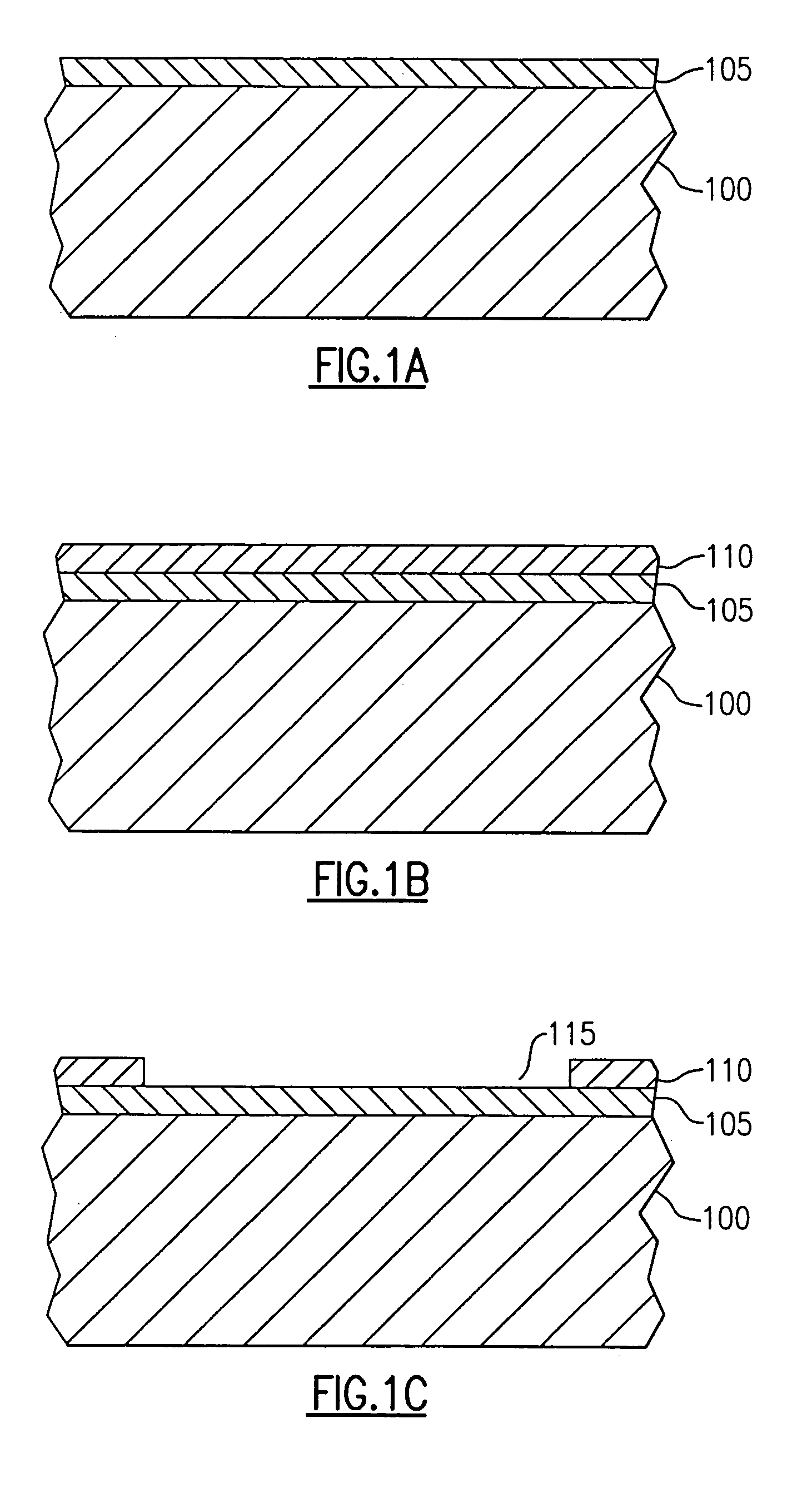
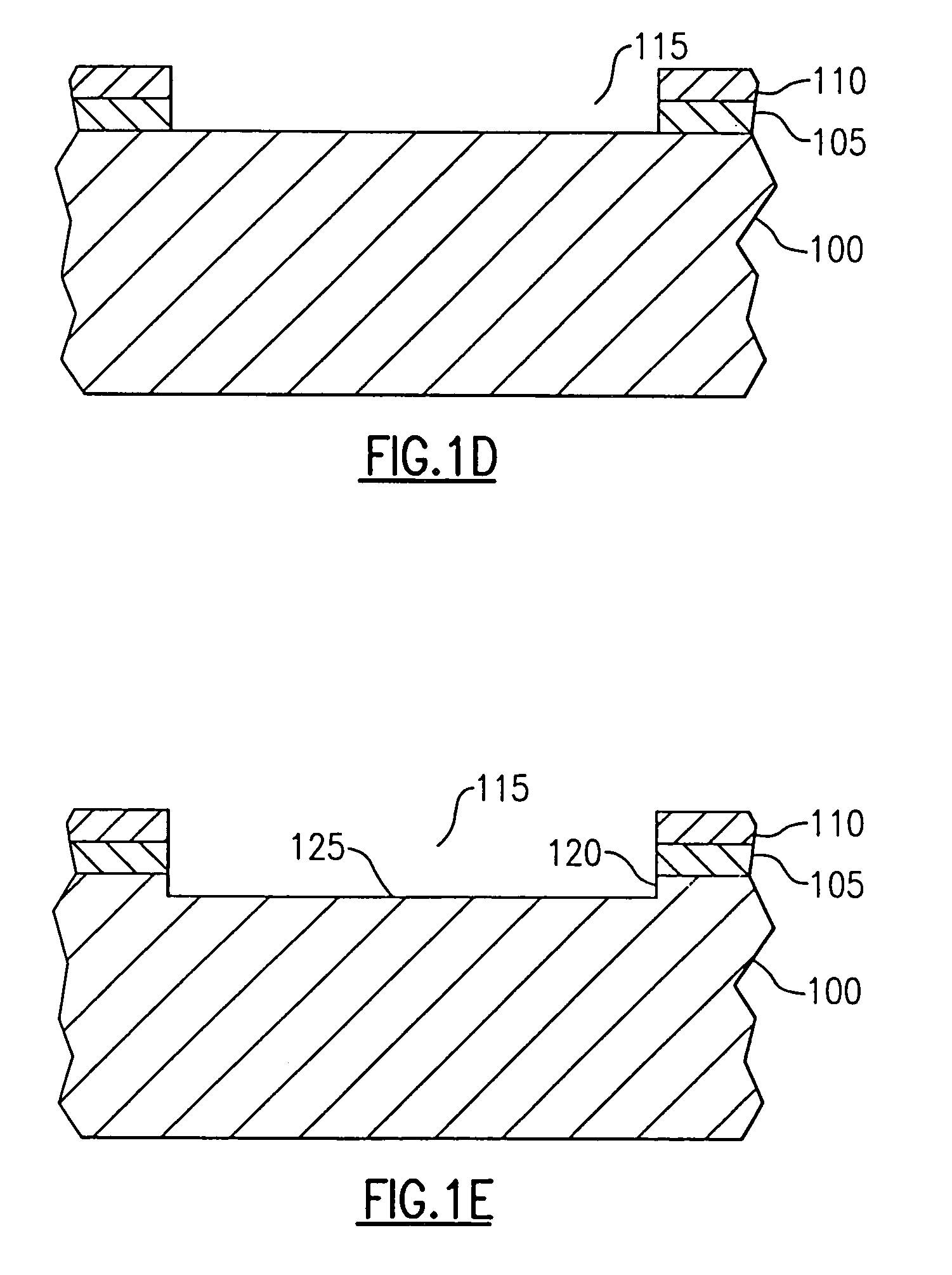
[0024]This method is compatible with either resist-masked etching or etching without resist mask. In one embodiment of the invention, silicon oxide is patterned as a mask over a silicon substrate, and an etch method selective for silicon oxide is employed on the patterned silicon wafer. The silicon oxide will be consumed at a much faster rate than the silicon according to well-established selectivity ratios. In this manner, by regulating the thickness of the silicon oxide mask, the exposed silicon can be etched with great precision.
[0031]The tops of the structures can be made to be co-planar with the field region (the preferred embodiment) so as to facilitate and ensure sealing to a bonded surface and to prevent formation of a fluidic “sneak path”. Alternatively, the structures can be fabricated such that their tops can be at the level of the shallower channel in a stepped channel. This is accomplished by appropriate segregation of the structure patterns between masks corresponding to the separate channel segments.
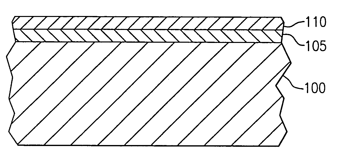
[0036]According to an embodiment of the invention, a method for etching an ultra-shallow channel includes the steps of providing a substrate of a first material; forming a layer of a second material on at least part of said first material; selectively removing a portion of said second material such that said second material is completely removed in at least one area to expose at least one area of said first material and is at least partially persistent in areas adjacent to said at least one exposed area of said first material so as to provide direct etchant communication with said first material within said at least one exposed area and to prevent etchant communication with said first material in areas where said second material has not been completely removed, and such that said act of removing said portion of said second material does not significantly remove any of said first material; providing an etch process that is selective for said second material and selective to said first material, wherein said etch process preferentially etches said second material at a rate that is significantly greater than that at which said etch process would etch said first material; and applying said etch process to etch said first material to a desired depth of said ultra-shallow channel.

Problems solved by technology

Any given etch process, to be effective, preferentially etches one material at a relatively fast rate, and is less effective in etching a second material that is simultaneously presented for etching.

Method used


Image

  • Fabrication of ultra-shallow channels for microfluidic devices and systems
  • Fabrication of ultra-shallow channels for microfluidic devices and systems
  • Fabrication of ultra-shallow channels for microfluidic devices and systems

Examples


Embodiment Construction

[0091]Reference will now be made in detail to the present exemplary embodiments of the invention, examples of which are illustrated in the accompanying drawings. Wherever possible, the same reference numbers will be used throughout the drawings to refer to the same or like parts.

[0092]The first principal aspect of the present invention addresses the formation of shallow and ultra-shallow fluid transport channels. “Shallow” as used herein means depths ranging from 1 μm to 10 μm. “Ultra-shallow” as used herein means depths below a micron ranging from 10 nm to 1000 nm (1 μm). “Standard” as used herein means depths ranging from 10 μm–100 μm, while “deep” means depths greater than 100 μm. One micron is chosen as the dividing line between shallow and ultra-shallow because conventional methods of fabrication do not work reliably below one micron.

[0093]Methods of fabrication are disclosed whereby sub-micrometer channel depths can be reproducibly created using standard semiconductor processi...


PUM

PropertyMeasurementUnit
Depthaaaaaaaaaa
Depthaaaaaaaaaa
Depthaaaaaaaaaa

Abstract

A method for etching an ultra-shallow channel includes using an etch process that is selective for one material to etch a different material in order to achieve a very precise channel depth in the different material. Channels as shallow as 10 nm can be fabricated in silicon with precision of 5 nm or better using the method. Stepped channels can be fabricated where each segment is a different depth, with the segments being between 10 nm and 1000 nm in depth. The method is applied to create a fluidic channel which includes a channel substrate to which is bonded a lid substrate to confine fluids to the fluidic channels so fabricated.

Description

CROSS-REFERENCE TO RELATED APPLICATIONS[0001]This application claims priority under 35 U.S.C. §119(e) based on U.S. Provisional Application Ser. No. 60 / 356,493 filed Feb. 12, 2002 and entitled FABRICATION OF SHALLOW AND ULTRA-SHALLOW CHANNELS FOR MICROFLUIDIC DEVICES AND SYSTEMS, incorporated herein by reference in its entirety.FIELD OF THE INVENTION[0002]This invention relates generally to the field of design, development and manufacturing of miniaturized chemical and biochemical analysis devices and systems using microelectromechanical systems (MEMS) technology, and more particularly to process sequences for fabricating MEMS and microfluidic devices and systems having fluid transport systems with any or all of the following attributes: (1) ultra-shallow depths; (2) well-controlled variations in channel depth; and (3) structures in the channels of sub-micrometer size.BACKGROUND OF THE INVENTION[0003]The creation of channels in a substrate at a microminiaturized scale has many poten...

Claims


Application Information

Patent Timeline
IPC IPC(8): F15C1/06H01L21/461B01F5/06B01F13/00B01J19/00B01L3/00B81B1/00B81C1/00G01N30/60
CPCB01F5/061B01F13/0059B01J19/0093B81C1/00071G01N30/6078B01F5/0644G01N30/6095B01F2005/0621B01J2219/00783B01J2219/00828B01J2219/00831B01J2219/00864B01J2219/00934B01L3/5027B81B2201/058B81B2203/0338B81B2203/0376Y10T137/2224Y10T137/0402B01F25/4317B01F25/4323B01F33/30
Inventor MOON, JAMES E.YOUNG, LINCOLN C.
Owner RHEONIX
Learn More