Electromagnetic wave detection arrangement with capacitive feedback

a capacitive feedback and electromagnetic wave technology, applied in the field of electromagnetic wave detection systems, can solve the problems of system integration time and detection sensitivity correlation, significant constraints on the size and power dissipation of sensors, and the quality of images and overall device costs,

Inactive Publication Date: 2007-02-06
MICROSOFT TECH LICENSING LLC
View PDF39 Cites 31 Cited by
  • Summary
  • Abstract
  • Description
  • Claims
  • Application Information

AI Technical Summary

Problems solved by technology

In medical applications, there are significant constraints on the size and power dissipation of sensors to allow insertion in the human body or, in general the use in a sterile environment.
In commercial video, generally the most stringent constraints are acquisition time, quality of the image and overall device cost.
One of the limitations of such systems is the apparent correlation between integration time and sensitivity of detection.
The spurious current from reset transistor 152 charges Cd and other parasitic capacitances at node VO resulting in a sampled error voltage.
Hence, a long integration time must be used to obtain a sufficiently strong signal, making this arrangement generally unsuitable for fast and dim EM waveforms.

Method used


Image

  • Electromagnetic wave detection arrangement with capacitive feedback
  • Electromagnetic wave detection arrangement with capacitive feedback
  • Electromagnetic wave detection arrangement with capacitive feedback

Examples


Embodiment Construction

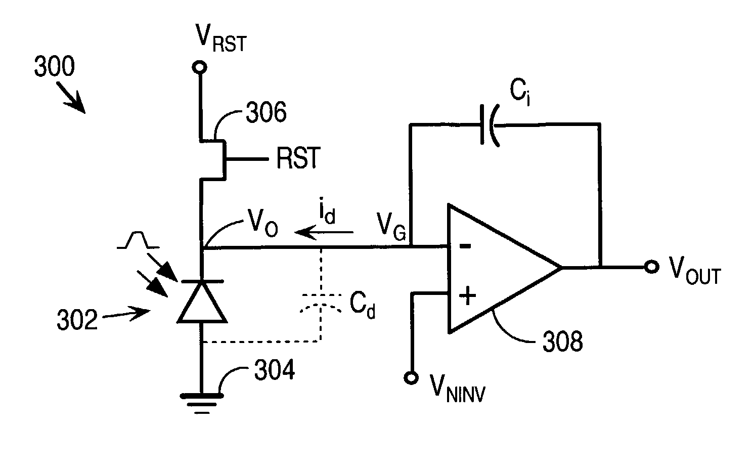
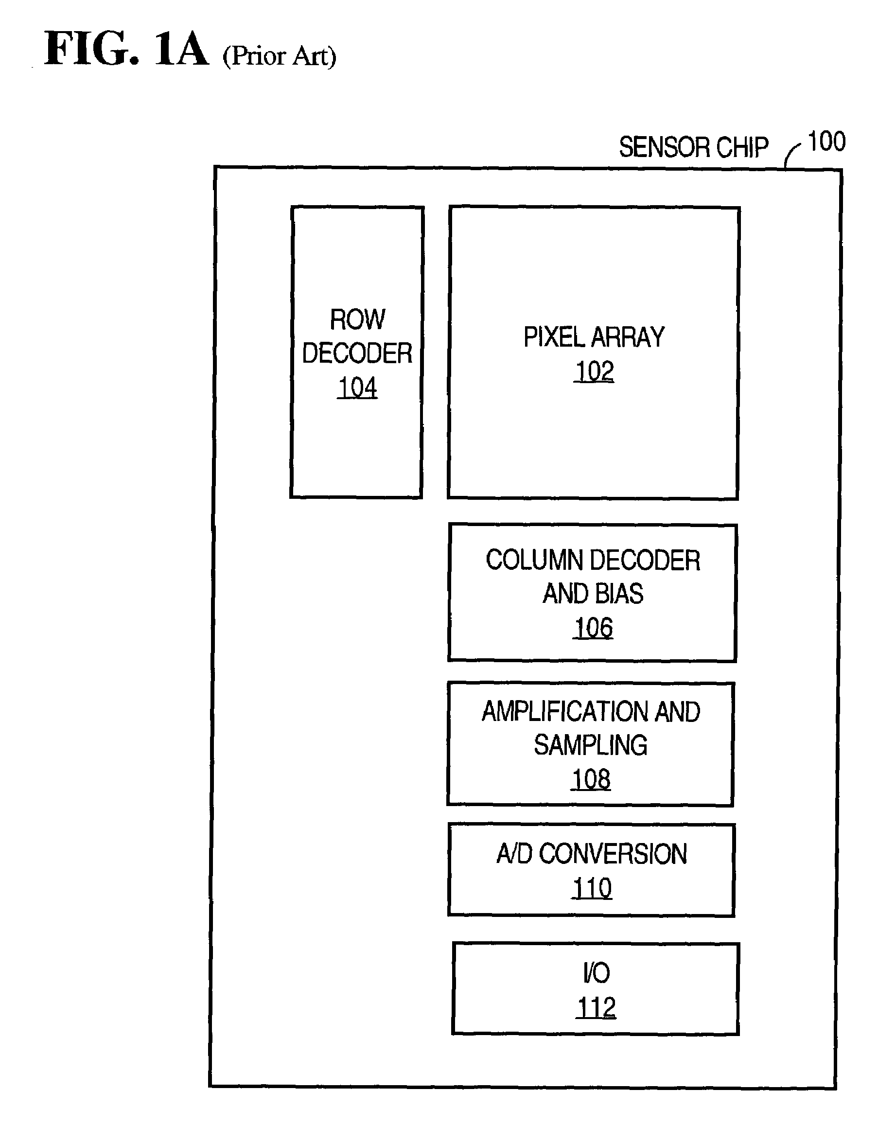
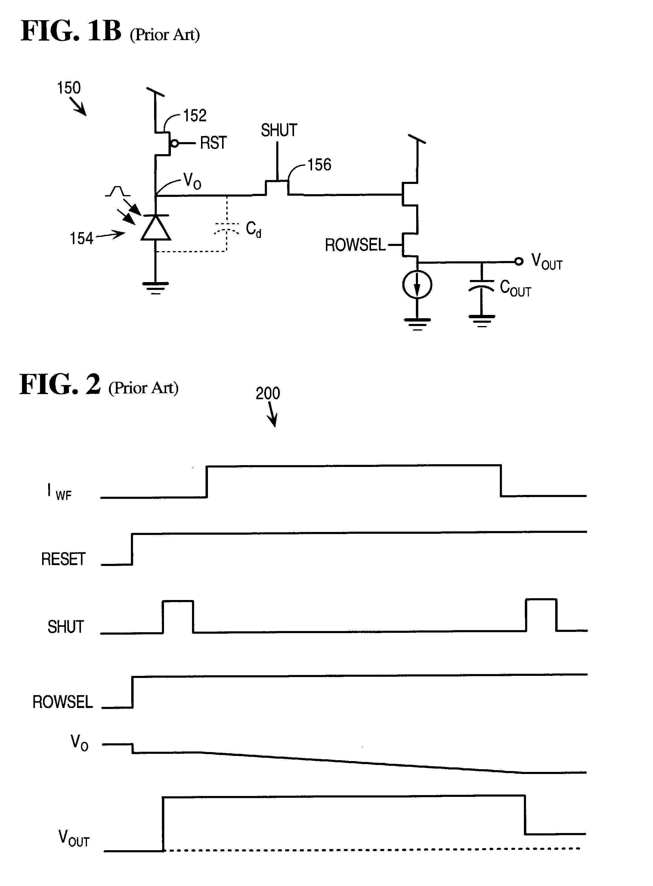
[0025]In the following description, for the purposes of explanation, specific details are set forth in order to provide a thorough understanding of the invention. However, it will be apparent that the invention may be practiced without these specific details. In some instances, well-known structures and devices are, depicted in block diagram form in order to avoid unnecessarily obscuring the invention. Various aspects and embodiments of the invention are described in the following sections: (1) overview; (2) capacitive feedback arrangements; (3) capacitance structures, (4) noise cancellation; (5) capacitive feedback combined with noise cancellation; and (6) implementation mechanisms.

1. Overview

[0026]An approach is provided for detecting EM waves using a photo detector coupled to an amplifier stage. The amplifier stage uses capacitive feedback to reduce or cancel intrinsic capacitance of the photo detector. A variety of capacitance structures may be used to provide the capacitive fee...


PUM


Abstract

An approach is provided for detecting EM waves using a photodetector coupled to an amplifier stage. The amplifier stage uses capacitive feedback to reduce or cancel intrinsic capacitance of the photodetector. A variety of capacitance structures may be used to provide the capacitive feedback such as shielded capacitors and capacitor arrays. The amplifier stage may be either single-ended or fully differential, depending upon the requirements of a particular application. Noise cancellation circuitry may also be included to reduce noise and offset sources present in the amplifier stage. The approach is applicable to a variety of contexts and applications. Example applications include, without limitation, detection of both brightness and Time of Flight (TOF) in 3D sensing applications. The approach may also be used to detect EM wave intensity in 2D sensing systems and, in general, for any application requiring simultaneously high speed and high sensitivity EM detection.

Description

RELATED APPLICATION[0001]This application claims priority from U.S. Provisional Patent Application No. 60 / 317,578, entitled “HIGH SENSITIVITY, HIGH SPEED, LOW NOISE CONVERSION TECHNIQUES FOR CMOS IMAGING,” filed Sep. 5, 2001 by Edoardo Charbon, the contents of which are incorporated herein by reference in their entirety for all purposes.FIELD OF THE INVENTION[0002]The invention relates to electromagnetic (EM) wave detection systems, and more specifically, to an approach for detecting EM waves that provides improved performance and reproducibility.BACKGROUND OF THE INVENTION[0003]Sensors for the detection of two-dimensional and three-dimensional images are used in numerous applications, such as commercial video, medical applications, astronomy and instrumentation. The particular type of EM wave detection employed varies depending upon the context and requirements of a particular application, such as wavelength and acquisition speed. For example, in astronomy, light images are extreme...

Claims


Application Information

Patent Timeline
Patent Type & Authority Patents(United States)
IPC IPC(8): H03F3/08G01J1/46H04N5/335H04N5/357H04N5/363H04N5/369H04N5/374
CPCG01J1/46H04N5/374H04N5/357H04N25/60H04N25/76H04N25/79
Inventor CHARBON, EDOARDO
Owner MICROSOFT TECH LICENSING LLC
Why Eureka
Try Eureka