Semiconductor device

a technology of semiconductor devices and semiconductors, applied in semiconductor devices, semiconductor/solid-state device details, electrical apparatus, etc., can solve the problems of increasing the potential for short circuit between the leads of neighboring transistors, and the inability to provide high breakdown voltage, so as to achieve high dielectric strength and increase the dielectric strength of resin

Active Publication Date: 2007-02-06
RENESAS ELECTRONICS CORP
View PDF2 Cites 38 Cited by
  • Summary
  • Abstract
  • Description
  • Claims
  • Application Information

AI Technical Summary

Benefits of technology

[0038](a) the means (1) has a structure in which the third lead (drain lead) of the first semiconductor chip protrudes from the second surface of the package and in which the seventh lead (drain lead) of the second semiconductor chip protrudes from the first surface of the opposite surface of the second surface of the package; further, since a lead is not arranged at the position of a lead terminal 6 between the first lead (source lead) of the first semiconductor chip of the package and the seventh lead (drain lead) of the second semiconductor chip, a gap between the first lead (source lead) and the seventh lead (drain lead) becomes wide; still further, since a lead is not arranged at the position of a lead terminal 2 between the third lead (drain lead) of the first semiconductor chip and the fifth lead (source lead) of the second semiconductor chip, a gap between the third lead (drain lead) and the fifth lead (source lead) becomes wide. With these, it is possible to prevent a short circuit from developing between the drain lead and the source lead adjacent to the drain lead and hence to increase the dielectric strength of the transistor formed in the first and the second semiconductor chip. For example, it is possible to make the dielectric strength between the source and the drain as large as the vicinity of 600 V.
[0039](b) The gap between the semiconductor chip fixing part and the respective leads whose tips face the semiconductor chip fixing part is as wide as from 0.3 mm to 0.7 mm. Hence, this can increase the dielectric strength of resin filled in the gap and forming the package. Therefore, it is possible to provide a semiconductor device having a high dielectric strength.BRIEF DESCRIPTION OF THE DRAWINGS

Problems solved by technology

For example, the above-described semiconductor device mounted with two transistor chips is required to have a breakdown voltage as high as 600 V. However, in now-available products, a gap between neighboring leads is as narrow as 0.87 mm and it turned out that the increasing of the breakdown voltage of the product results in increasing a potential that a short circuit might develop between the leads of neighboring transistors and hence in making it impossible to provide a high breakdown voltage by the present structure.

Method used


Image

  • Semiconductor device
  • Semiconductor device
  • Semiconductor device

Examples


embodiment 1

[Embodiment 1]

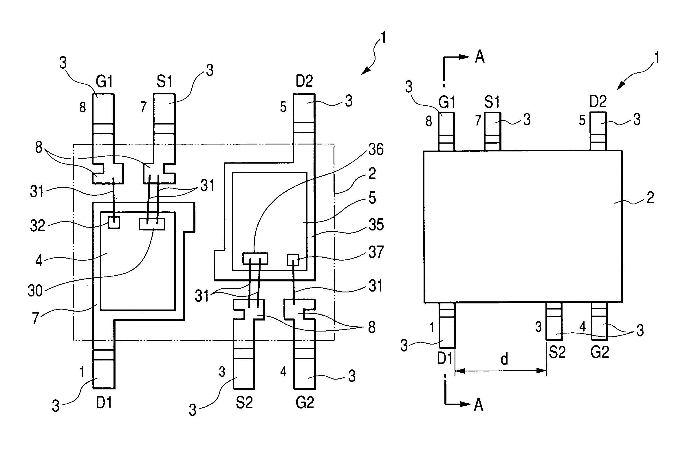
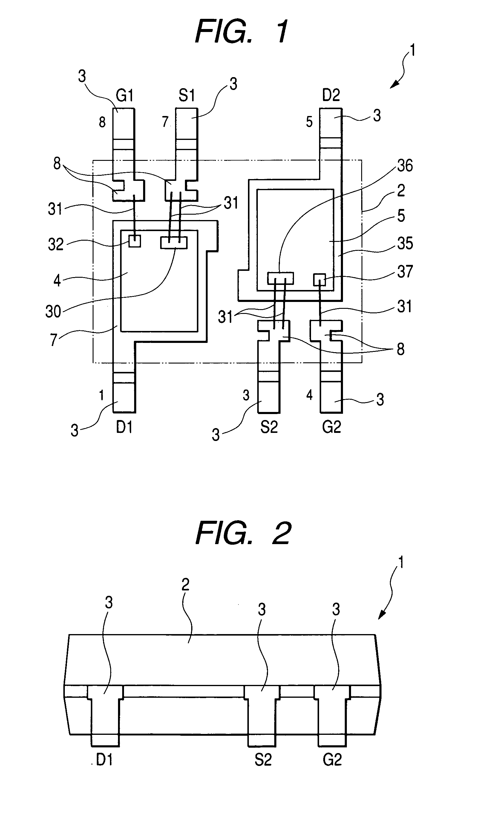
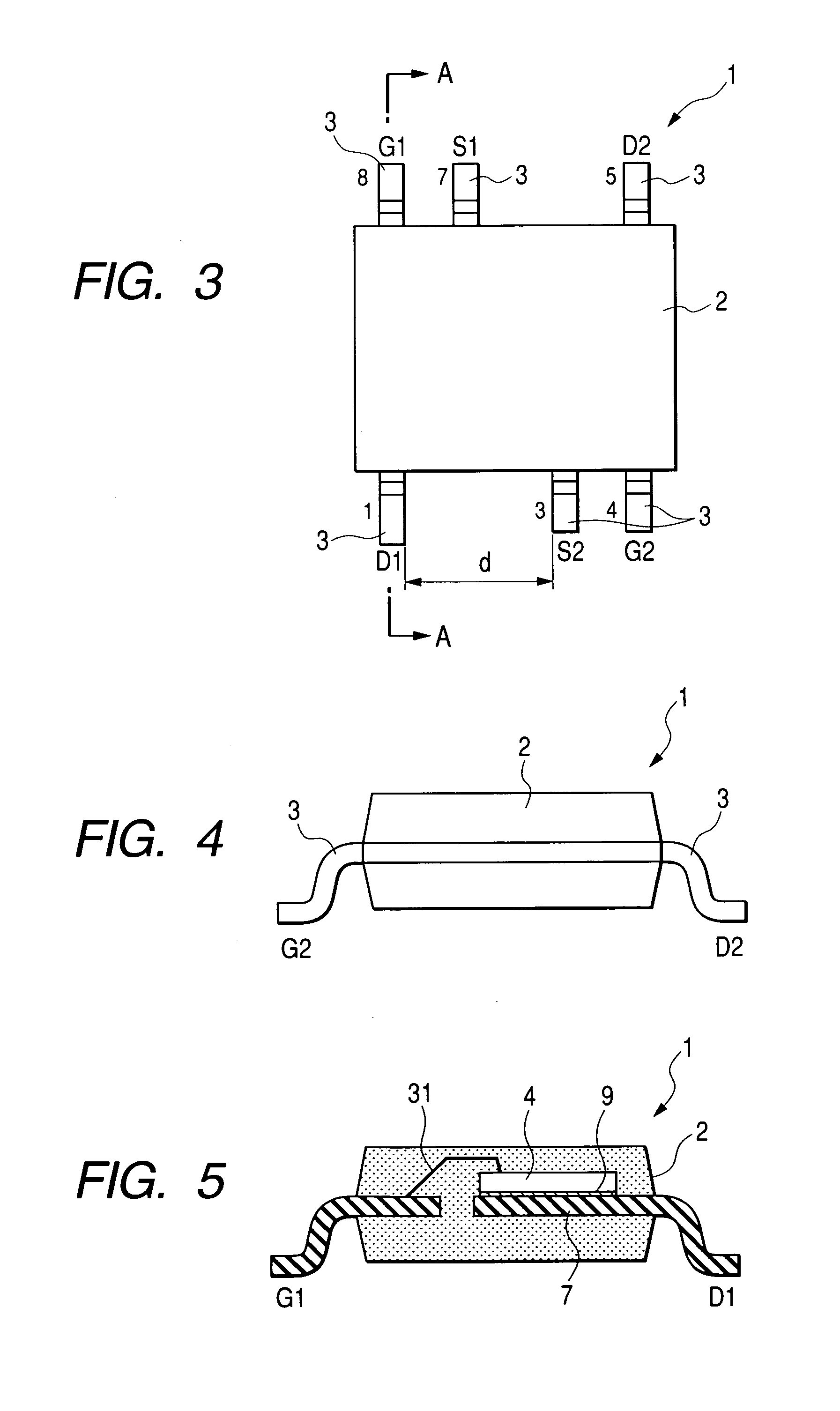
[0065]In this embodiment will be described an example of applying the invention to a semiconductor device having a construction in which two semiconductor chips (the first semiconductor chip and the second semiconductor chip) each having a transistor formed therein are packaged in a single package. In this embodiment 1, an example of a semiconductor chip having a vertical type power MOSFET formed therein will be described. The semiconductor device like this can be used as a constituent part of, for example, a DC-DC converter circuit. Of the two transistors (the first transistor and the second transistor), one is a switching transistor and the other is a rectifier transistor.

[0066]FIGS. 1 to 14 are illustrations related to a semiconductor device of this embodiment 1. FIGS. 1 to 7 are illustrations related to the structure of the semiconductor device. FIG. 8 is an illustration to shown a mounting state. FIG. 9 is a bridge circuit diagram in which the semiconductor device...

embodiment 3

[Embodiment 3]

[0105]FIG. 16 and FIG. 17 are illustrations related to a semiconductor device of embodiment 3 of the invention. FIG. 16 is a schematic plan view to show in a transparent state the semiconductor chip fixing part and inner leads in the package in the semiconductor device. FIG. 17 is a schematic enlarged sectional view to show a portion of a semiconductor chip used for the semiconductor device.

[0106]In the semiconductor device 1 of the embodiment 1, the transistors of the semiconductor chips 4, 5 are N-channel type vertical MOSFET. In the semiconductor device 1 of this embodiment 3, the transistor of the semiconductor chip 4 is an N-channel type vertical MOSFET (Nch) and the other structure is the same as the semiconductor device 1 of the embodiment 1 except that the transistor of the semiconductor chip 5 is a P-channel type vertical MOSFET.

[0107]FIG. 17 shows an illustration to show the cell portion of the P-channel type vertical MOSFET. The P-channel type vertical MOSFE...

embodiment 4

[Embodiment 4]

[0109]FIG. 18 and FIG. 19 are illustrations related to a semiconductor device of embodiment 4 of the invention. FIG. 18 is a schematic plan view to show in a transparent state the semiconductor chip fixing part and inner leads in the package in the semiconductor device. FIG. 19 is a bridge circuit of an electronic device in which the semiconductor device of the embodiment 4 is built.

[0110]The semiconductor device 1 of this embodiment 4 is different from the semiconductor device 1 of the embodiment 1 in a structure that the semiconductor chip fixing part 7 is connected to the semiconductor chip fixing part 35 by a connection part 60. Further, another different point is that the semiconductor chip 4 made of the P-channel type vertical MOSFET (Pch) is fixed on the semiconductor chip fixing part 7 and that the semiconductor chip 5 made of the N-channel type vertical MOSFET (Nch) is fixed on the semiconductor chip fixing part 35. The other portions are the same as those in ...


PUM


Abstract

A semiconductor device includes: a package; two semiconductor chip fixing parts located adjacently to each other in the package; and first and the second semiconductor chips, each of which is fixed on the semiconductor chip fixing part and has a field effect transistor formed therein. A gate lead G1, a source lead S1, and a drain lead D2 are arranged from left to right on the first surface of the package and a drain lead D1, a source lead S2, and a gate lead G2 are arranged from left to right on the second surface. A gap between the source lead S1 and the drain lead D2 is two times a gap between the gate lead G1 and the source lead S1, and a gap between the drain lead D1 and the source lead S2 is two times a gap between the source lead S2 and the gate lead G2.

Description

BACKGROUND OF THE INVENTION[0001]1. Field of the Invention[0002]The present invention relates to a semiconductor device and an electronic device and a technology effectively applied to, for example, a semiconductor device that has a plurality of semiconductor chips, each of which has a transistor formed therein, in a package and has a high breakdown voltage.[0003]2. Description of the Related Art[0004]As one of the semiconductor devices has been known a semiconductor device having a structure (so-called SOP8 type) in which two semiconductor chips each having a transistor formed therein is mounted in a package and in which four leads are protruded from each side of one pair of sides opposite to each other of the package (for example, JPA-2000-217416).[0005]A plurality of power MOS FETs are used for a motor control, a power supply, and the like. A composite power MOS FET (transistor) studied by the inventors includes two power MOS FETs. FIGS. 21 to 24 are illustrations related to a co...

Claims


Application Information

Patent Timeline
Patent Type & Authority Patents(United States)
IPC IPC(8): H01L23/34H01L23/495H01L29/80H01L31/0328H01L25/07H01L25/18
CPCH01L23/49562H01L24/06H01L24/49H01L23/49575H01L2924/01033H01L24/45H01L2224/05553H01L2224/05647H01L2224/0603H01L2224/45144H01L2224/48095H01L2224/48247H01L2224/49111H01L2224/49171H01L2224/73265H01L2924/01004H01L2924/01005H01L2924/01006H01L2924/01014H01L2924/01015H01L2924/01029H01L2924/01047H01L2924/01078H01L2924/01079H01L2924/01082H01L2924/014H01L2924/13091H01L2924/1305H01L2924/1306H01L2224/48647H01L24/48H01L2224/32245H01L2924/01023H01L2924/00014H01L2924/00H01L2924/00012H01L2224/05554H01L2924/181H01L24/73
Inventor HATA, TOSHIYUKIKANAZAWA, TAKAMITSUOTANI, TAKESHI
Owner RENESAS ELECTRONICS CORP
Why Eureka
Try Eureka