Ground pad structure for preventing solder extrusion and semiconductor package having the ground pad structure

a ground pad and solder extrusion technology, which is applied in the direction of final product manufacturing, sustainable manufacturing/processing, semiconductor/solid-state device details, etc., can solve the problems of poor grounding ability and not only time-consuming, and achieve excellent grounding ability

Active Publication Date: 2007-02-06
SILICONWARE PRECISION IND CO LTD
View PDF8 Cites 107 Cited by
  • Summary
  • Abstract
  • Description
  • Claims
  • Application Information

AI Technical Summary

Benefits of technology

[0014]It is therefore an objective of this invention to provide a ground pad structure for preventing solder extrusion and a semiconductor package having the ground pad structure, which is capable of maintaining a good grounding quality and diminishing the occurrence of the electrical bridging among the adjacent conductive traces.
[0017]Since the ground pad structure of the present invention is capable of keeping the ground plane as a complete and continuous plate-shaped plane, an excellent grounding ability is thereby well maintained. In the meantime, while the ground pads located along the circumference of the ground plane being formed in a non-solder mask defined manner, the occurrence of unfavorable shorts due to the electrical bridging among the adjacent conductive traces can be avoided as the extrusion of the molten solder bumps from the ground pads located along the ground pad structure's circumference toward their adjacent conductive traces is effectively prevented.

Problems solved by technology

However, the non-solder mask defined ground pad 108b is not only time-consuming in its fabrication, but also leads to a poor grounding ability since the non-solder mask defined ground pad 108b is connected to the ground plane 108 merely by a pair of tiny tie bars 108c.

Method used


Image

  • Ground pad structure for preventing solder extrusion and semiconductor package having the ground pad structure
  • Ground pad structure for preventing solder extrusion and semiconductor package having the ground pad structure
  • Ground pad structure for preventing solder extrusion and semiconductor package having the ground pad structure

Examples


Embodiment Construction

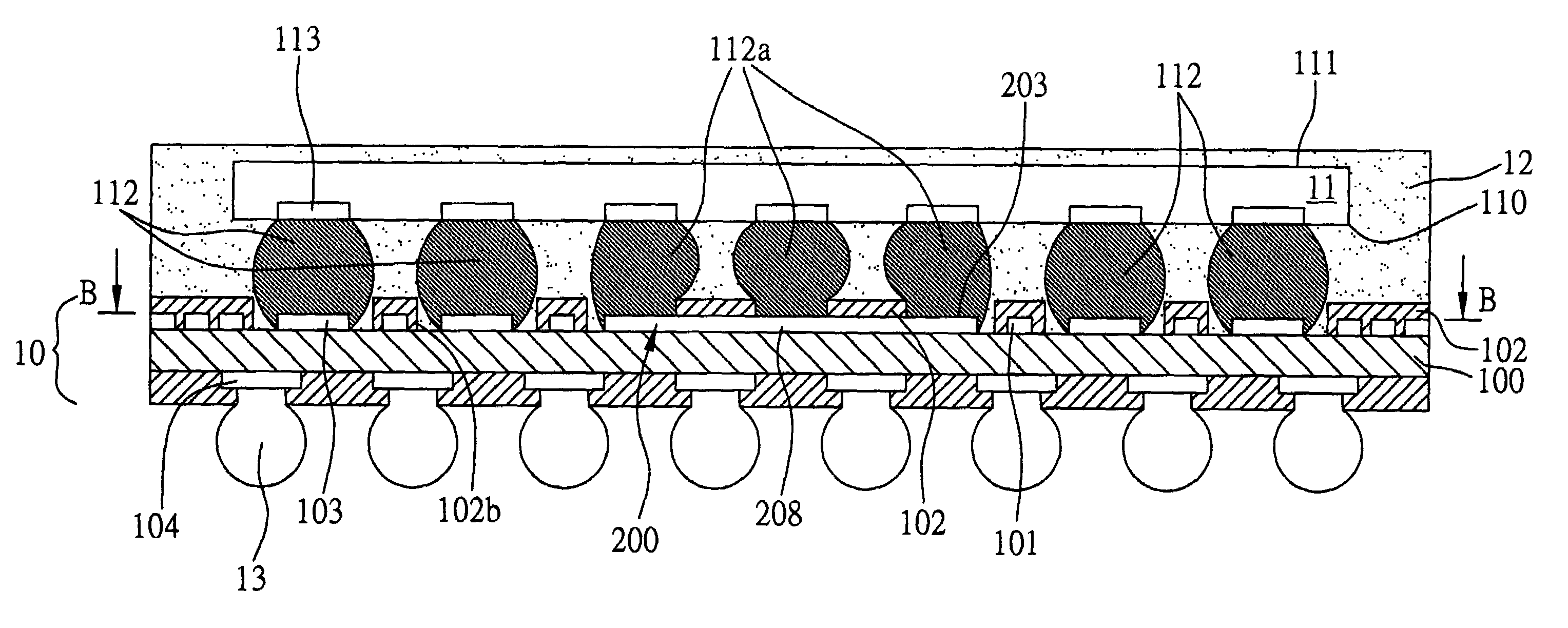
[0028]Preferred embodiments of the ground pad structure for preventing solder extrusion and the semiconductor package having the ground pad structure of the invention are disclosed in full details in the following with reference to FIGS. 7–9. However, instead of showing a real operative scheme in detail, the drawings depicting the embodiments illustrate merely the constituent parts related to the embodiments. It is to be noted that the semiconductor package of the invention will be more complex in its whole layout and with more details in the size and number of its components while in the real operative scheme.

[0029]Referring to FIG. 7, the ground pad structure 200 for preventing solder extrusion of the invention comprises a ground plane 208 that is made of conductive materials, and the shape of the ground plane 208 may be formed in a square as shown in FIG. 7 or any other preferred shape to fit a given occasion. The ground plane 208 is to be provided on an insulative dielectric lay...


PUM


Abstract

A ground pad structure for preventing solder extrusion and a semiconductor package having the ground pad structure are disclosed, wherein the ground pad structure has the ground pads located along the circumference of its ground plane be formed in a non-solder mask defined manner. Accordingly, a good grounding quality is maintained, and the occurrence of the electrical bridging among the adjacent conductive traces can be avoided as the extrusion of the molten solder bumps from the ground pads located along the ground pad structure's circumference toward their adjacent conductive traces is effectively prevented.

Description

BACKGROUND OF THE INVENTION[0001]1. Field of the Invention[0002]This invention relates to a ground pad structure for preventing solder extrusion and a semiconductor package having the ground pad structure, and more particularly, to a surface mount technology that can be used in a flip-chip ball grid array (FCBGA) package structure to enhance the bonding reliability of the chip by modifying the formation of the ground ball pads.[0003]2. Description of Related Art[0004]A semiconductor chip is capable of being electrically connected to a substrate or a printed circuit board through a plurality of conductive metal solder means, such as solder balls or solder bumps being arranged in a matrix array, and is thereby packaged into a semiconductor package, such as a ball grid array (BGA) package, in a manner of the flip-chip formation.[0005]The surface of the substrate is covered with an insulative solder mask layer while the chip is mounted in a flip-chip manner onto the substrate. A plurali...

Claims


Application Information

Patent Timeline
Patent Type & Authority Patents(United States)
IPC IPC(8): H05K1/11H01L23/498H01L23/50H05K3/28H05K3/34
CPCH01L23/49816H01L23/49838H01L23/50H05K1/111H05K3/3452H01L23/49822H01L2224/16238H01L2924/15311H05K3/284H05K3/3436H05K2201/093H05K2201/09381H05K2201/0989H05K2201/099H05K2201/10674H01L2924/01087H01L2224/16106H01L2224/05571H01L2224/05573H01L2224/056H01L2224/17106H01L24/17H01L2224/16237H01L2224/17051H01L24/05Y02P70/50H01L2224/17104H01L2924/00012H01L2924/00014
Inventor LIN, YING-RENHUANG, CHIH-MINGTSAI, HO-YI
Owner SILICONWARE PRECISION IND CO LTD
Why Eureka
Try Eureka