Guided wave spatial filter

a spatial filter and waveguide technology, applied in the direction of optical waveguide light guide, instruments, optics, etc., can solve the problems of quasi-chaotic perturbation of circuit characteristics, and achieve the effects of enhancing the extinction ratio, hindering the propagation and preventing the coupling of higher-order mode radiation

Inactive Publication Date: 2007-02-06
LUMENTUM TECH UK LTD
View PDF14 Cites 18 Cited by
  • Summary
  • Abstract
  • Description
  • Claims
  • Application Information

AI Technical Summary

Benefits of technology

[0035]The filter provides the benefit that higher-order mode radiation injected into the input waveguide, for example resulting from a misaligned fibre waveguide connected to the input waveguide, does not interfere with operation of the splitter, the splitter thereby being desensitised to higher-order mode radiation components input to the splitter.
[0036]In the splitter, it is beneficial that at least one of the output waveguides is connected to the mixing region through a spatial filter according to the first aspect of the invention, the filter operable to hinder coupling of higher-order mode radiation from the mixing region into said at least one of the output waveguides. Inclusion of the filter at the output waveguides assists to prevent higher-order mode radiation excited within the mixing region being coupled down-stream to other optical devices connected to the splitter.
[0037]In a third aspect of the present invention, there is provided an optical modulator incorporating modulating means for selectively diverting radiation input to the means between a plurality of output paths in response to a control signal applied to the means, at least one of the output paths including a filter according to the first aspect of the present invention for transmitting fundamental mode radiation output from the means to said at least one of the output paths and for hindering propagation of higher-order mode radiation from the means to said at least one of the output paths.
[0038]It is preferable that the modulating means and output paths are implemented in rib-waveguide form, the modulating means and the filter being flanked by regions which are sufficiently deeply etched to render them unsusceptible to propagating higher-order mode radiation therethrough. The relatively deeply etched regions are effective at containing radiation and thereby providing the modulator with an enhanced extinction ratio.
[0039]When designing the modulator to be compact, it is beneficial that at least one of the output paths includes a faceted rib waveguide boundary where the path adjoins onto the modulating means, inclusion of the boundary enabling the path to project directly away from the modulating means at a greater angle than possible without the faceted boundary. Such a greater angle enables the modulator in microfabricated form to be shorter.
[0040]In order to desensitise the modulator to higher-order mode radiation injected thereinto, the modulator preferably comprises an input path for injecting radiation into the modulating means, the input path connected through a filter according to the first aspect of the invention, the filter operable to transmit fundamental mode radiation from the input path to the modulating means and to hinder higher-order mode radiation being injected from the input path to the modulating means.

Problems solved by technology

Such coherent interaction often results in a quasi-chaotic perturbation to characteristics of the circuit because the fundamental mode radiation and the higher-order mode radiation possess different characteristic propagation velocities and therefore different relative phases at a downstream interaction zone within the integrated circuit.

Method used


Image

  • Guided wave spatial filter
  • Guided wave spatial filter
  • Guided wave spatial filter

Examples


first embodiment

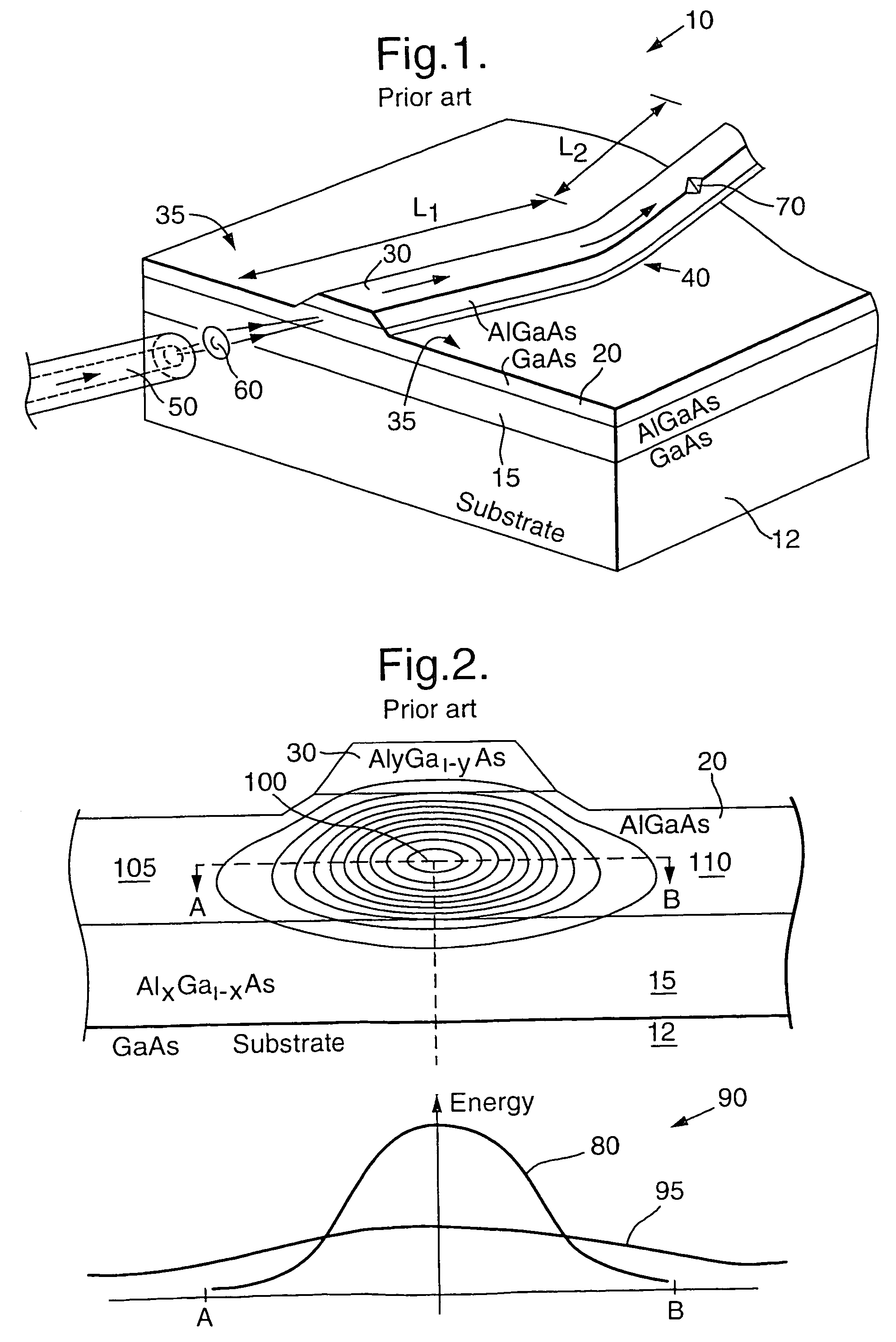
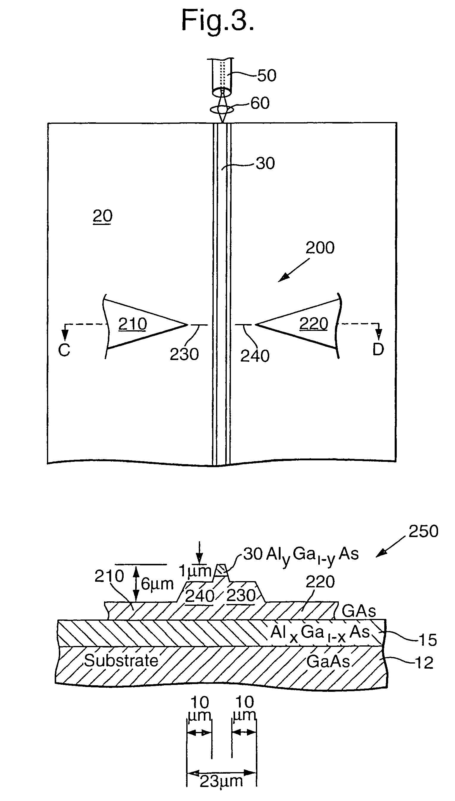
[0081]Referring now to FIG. 3, there is shown in plan view a pin-hole type guided wave spatial filter according to the invention. The pin-hole filter is indicated generally by 200 and includes the substrate 12, the lower substrate layer 15, the upper substrate layer 20, the rib waveguide 30 and two deeper etch regions 210, 220 etched symmetrically about the waveguide 30 but not encroaching thereonto; regions of shallower etching 230, 240 separate the waveguide 30 from the deeper etch regions 210, 220. The deeper regions 210, 220 each assume the form of a triangular area having a corner thereof orientated to point towards the waveguide 30 as illustrated in FIG. 3, each corner is at a distance of 10 μm from its nearest peripheral wall of the waveguide 30. The comers are mutually separated by a distance of substantially 23 μm.

[0082]In FIG. 3, there is also shown a cross-sectional view of the filter 200 along an axis C–D, the view indicated generally by 250.

[0083]When fabricating the fi...

second embodiment

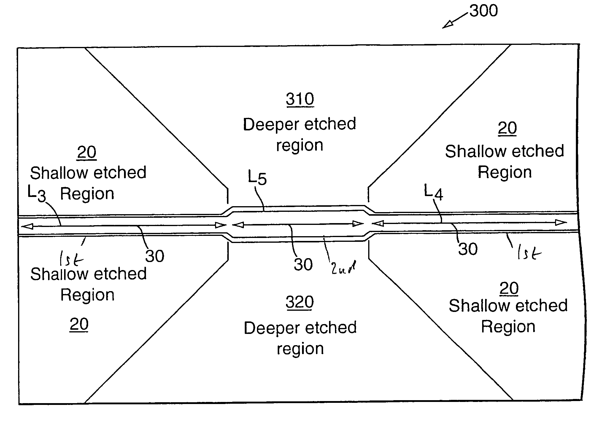
[0097]The inventor has therefore devised an alternative design of spatial filter according to the invention which addresses the performance limitations of the filter 200 as well as technical difficulties associated with its fabrication. Referring to FIG. 4, there is shown in plan view an in-line type guided wave spatial filter according to the invention, the in-line guided wave filter indicated generally by 300. The filter 300 comprises the waveguide 30 flanked along its length in sections L3, L4 thereof by the upper substrate layer 20 which has been shallowly etched back so that an upper surface of the waveguide remotest from the layer 20 projects 1 μm above the layer 20 in a similar manner as in the integrated circuit 10. The filter 300 additionally comprises a central section L5 situated between the section L3, L4 where the waveguide 30 is flanked by deeper etch regions 310, 320 at both sides thereof These deeper regions 310, 320 both taper outwardly away from the waveguide 30; a...

third embodiment

[0111]Variants of the spatial filter 300 in FIG. 5 can be fabricated in conjunction with other types of optical structures, for example FIG. 8 is an illustration of a multimode interference splitter indicated generally by 800, the splitter 800 comprising a guided wave spatial filter indicated by 810 according to the invention incorporated at an optical input port of the splitter 800.

[0112]In comparison to the splitter 800, a conventional multimode splitter comprises an optical input port coupled to a multimode mixing region including a plurality of optical output ports. The input and output ports are coupled to waveguides for guiding optical radiation to and from the mixing region. Fundamental mode input radiation is applied through a waveguide associated with the input port to the mixing region and excites a multiplicity of radiation modes in the region. The output ports are judicially positioned where the multiplicity of modes mutually sum to provide energy maxima. As a consequenc...


PUM

PropertyMeasurementUnit
free-space wavelengthaaaaaaaaaa
heightaaaaaaaaaa
heightaaaaaaaaaa

Abstract

The invention concerns a guided wave spatial filter (300) for receiving input radiation and outputting corresponding filtered output radiation, the filter comprising first and second waveguide sections (30, L3, L5) connected in series, the sections: (a) mutually matched for transmitting fundamental mode radiation components present in the input radiation therethrough to provide the output radiation; and (b) mutually mismatched for hindering higher-order mode radiation components present in the input radiation from propagating therethrough and contributing to the output radiation. The spatial filter (300) is implemented using rib waveguides (30) for the sections with associated relatively deeply and relatively shallowly etched structures (20, 310, 320) for imparting to the sections their radiation mode filtration characteristics. The spatial filter according to the invention can be incorporated into optical splitters and optical modulators to enhance their performance and desensitise them to higher-order mode radiation injected thereinto.

Description

RELATED APPLICATIONS[0001]This application is a 35 U.S.C. 371 national stage filing of International Application No. PCT / GB01 / 04479, filed 8 Oct. 2001, which claims priority to Great Britain Patent Application No. 0024670.2, filed on 9 Oct. 2000 in Great Britain. The contents of the aforementioned applications are hereby incorporated by reference.BACKGROUND OF THE INVENTION[0002]The present invention relates to a guided wave spatial filter, in particular but not exclusively to a guided wave spatial filter suitable for use in conjunction with rib waveguides in optical integrated circuits.[0003]For the purposes of describing the present invention, optical radiation is defined as radiation having a free-space wavelength in a range of 100 nm to 15 μm.[0004]Monolithic optical integrated circuits are well known. They are described in a publication “Introduction to Semiconductor Integrated Optics” by H P Zappe (ISBN 0-89006-789-9, Artech House Publishers 1995). A conventional optical integ...

Claims


Application Information

Patent Timeline
Patent Type & Authority Patents(United States)
IPC IPC(8): G02B6/10G02B6/26G02B6/12G02B6/122G02B6/125G02B6/136G02B6/14G02B6/28G02F1/015G02F1/025G02F1/313
CPCG02B6/125G02B6/136G02B6/14G02B2006/12178G02B2006/12097G02B2006/12109G02B2006/12173G02B6/2813
Inventor WALKER, ROBERT GRAHAM
Owner LUMENTUM TECH UK LTD
Why Eureka
Try Eureka