

External volume insensitive flow verification
a flow verification and external volume technology, applied in the field of external volume insensitive flow verification, can solve the problems of time-consuming setup calibration, measurement errors, and ah error in gas flow rate, and achieve the effect of fast and accurate flow measurement and small siz
- Summary
- Abstract
- Description
- Claims
- Application Information
AI Technical Summary
Benefits of technology
Problems solved by technology
Method used
Image

Examples
Embodiment Construction
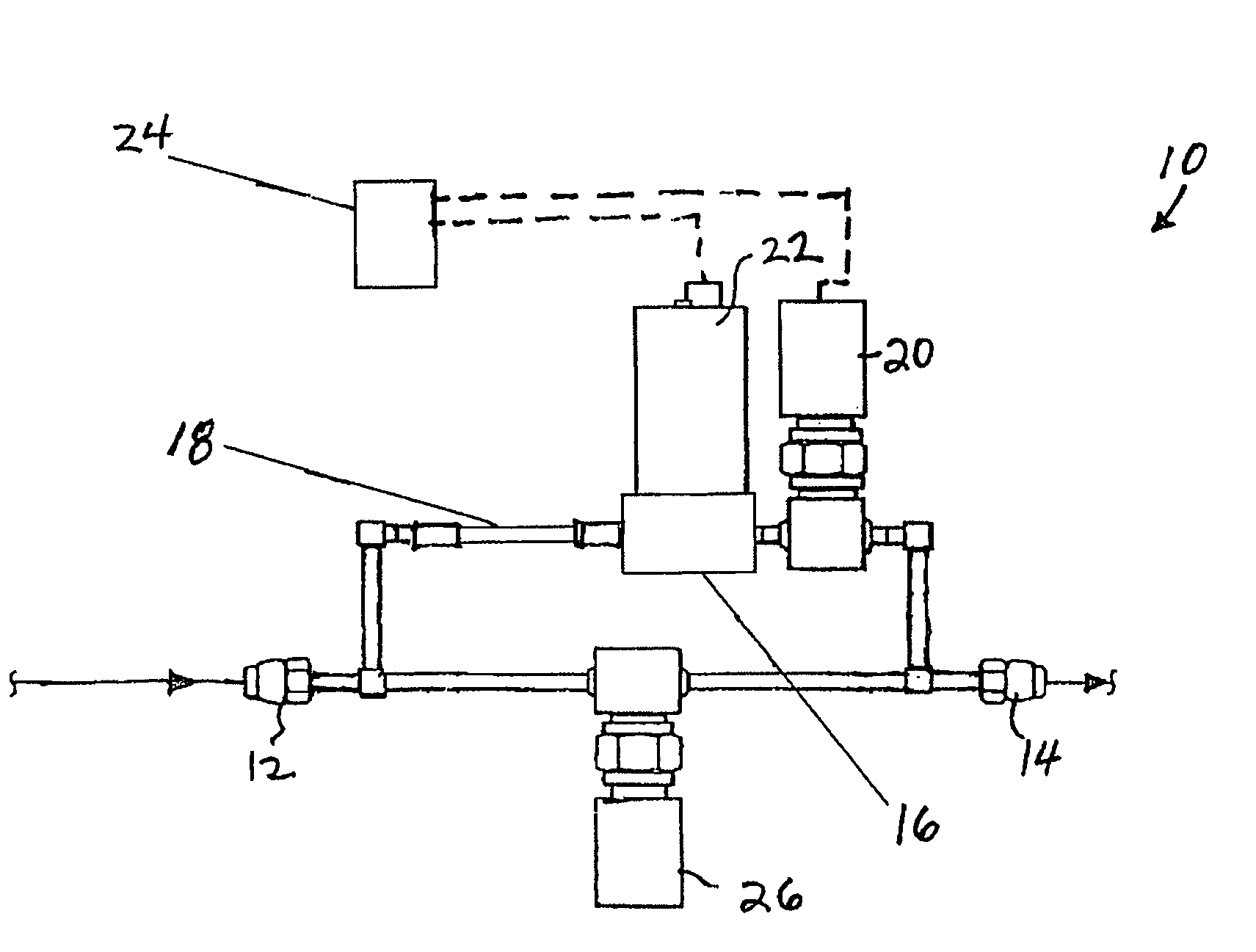
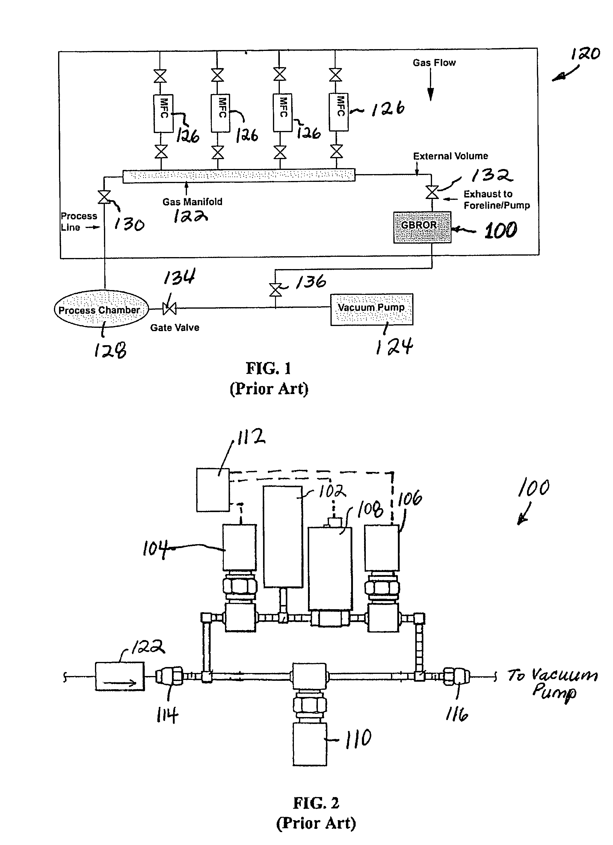
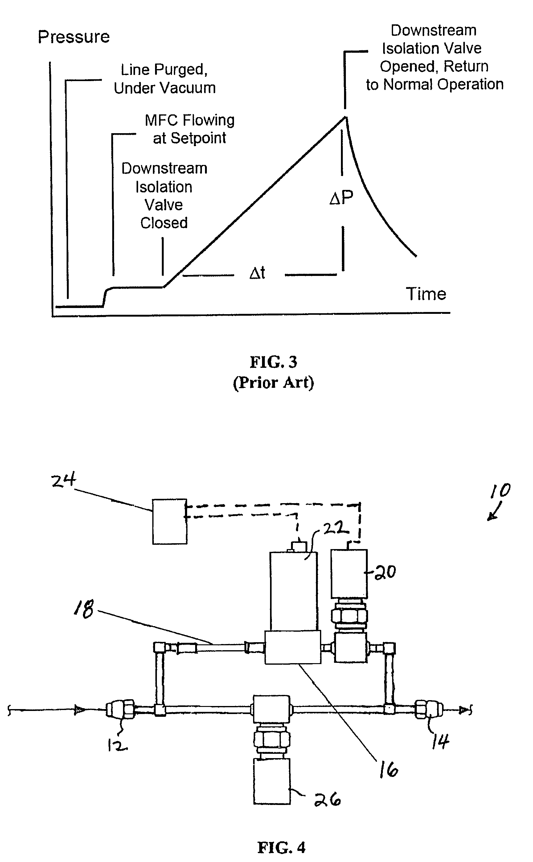
[0024]The present disclosure provides a rate-of-rise (ROR) mass flow verifier 10 and a method 40 for in-situ ROR mass flow verification and, if desired, calibration of a device-under-test (DUT), such as a mass flow controller (MFC). FIG. 4 shows an exemplary embodiment of the flow verifier 10 of the present disclosure, while FIG. 5 shows an exemplary embodiment of the method 40 of the present disclosure. The flow verifier 10 and method 40 of the present disclosure are particularly for use with gas metering systems for delivering contaminant-free, precisely metered quantities of process and purge gases to a semiconductor process chamber(s). The flow verifier 10 and method 40 provide in-situ verification of DUTs, and are substantially insensitive to the size of external (connecting) volumes.
[0025]Referring to FIG. 4, the exemplary embodiment of the mass flow verifier 10 includes an inlet 12 connectable to a DUT, and an outlet 14 connectable to a vacuum pump for drawing gas through the...
PUM
| Property | Measurement | Unit |
|---|---|---|
| temperature | aaaaa | aaaaa |
| pressure | aaaaa | aaaaa |
| pressure | aaaaa | aaaaa |
Abstract
Description
Claims
Application Information