Light-emitting semiconductor device having a quantum well active layer, and method of fabrication

a technology of light-emitting semiconductors and active layers, applied in semiconductor/solid-state device manufacturing, semiconductor devices, electrical devices, etc., can solve the problems of mutual diffusion of indium, well-layered deterioration in crystallinity, and difficulty and inconvenience, so as to prevent indium evaporation, reduce the amount of aluminum, and reduce the effect of resistan

Inactive Publication Date: 2007-02-13
SANKEN ELECTRIC CO LTD
View PDF10 Cites 25 Cited by
  • Summary
  • Abstract
  • Description
  • Claims
  • Application Information

AI Technical Summary

Benefits of technology

[0010]Made from an aluminum-nitride-based semiconductor, the second complementary sublayer functions to prevent the evaporation of indium and other ingredients from the well sublayer, and the mutual diffusions of indium from the well sublayer and gallium from the barrier sublayer. The first complementary sublayer of similar, but not necessarily identical, composition also serves the prevent the mutual diffusions of indium from the well sublayer and gallium from the barrier sublayer. The result is a significant improvement in the crystallinity of the active layer.
[0012]In order to prevent indium evaporation and diffusion from the well layer or layers while the active layer as a whole is held relatively low in resistivity, the second complementary sublayer or sublayers may be made greater in aluminum content than the first complementary sublayer or sublayers. Generally, the higher the aluminum proportions a and a′ of the AlaGabIn1-a-bN first complementary sublayer or sublayers and Ala′Gab′In1-a′-b′N second complementary sublayer or sublayers, the better will they reduce indium evaporation and diffusion. However, the first and second complementary sublayers will become more resistive as they grow higher in aluminum contents. As a compromise, and particularly in cases where the prevention of indium evaporation is more important, the second complementary sublayer or sublayers should be made as aforesaid greater in aluminum content than the first complementary sublayer or sublayers. This is believed to be the most practical solution to the problems of indium evaporation and indium and gallium diffusion.

Problems solved by technology

The resulting barrier layers have not necessarily been satisfactory in crystallinity, bringing about some difficulties and inconveniences set forth hereinbelow.
The barrier layers of poor crystallinity are, first of all, incapable of sufficiently restricting the vaporization of indium from the well layers, thereby allowing the well layers to deteriorate in crystallinity, too.
Another inconvenience is the mutual diffusions of indium from the well layers and gallium from the barrier layers, beyond the interfaces between the well and barrier layers.
The well layers have thus been easy to become irregular in virtual thickness, resulting in fluctuations in the wavelength of the light emitted.

Method used


Image

  • Light-emitting semiconductor device having a quantum well active layer, and method of fabrication
  • Light-emitting semiconductor device having a quantum well active layer, and method of fabrication
  • Light-emitting semiconductor device having a quantum well active layer, and method of fabrication

Examples


Embodiment Construction

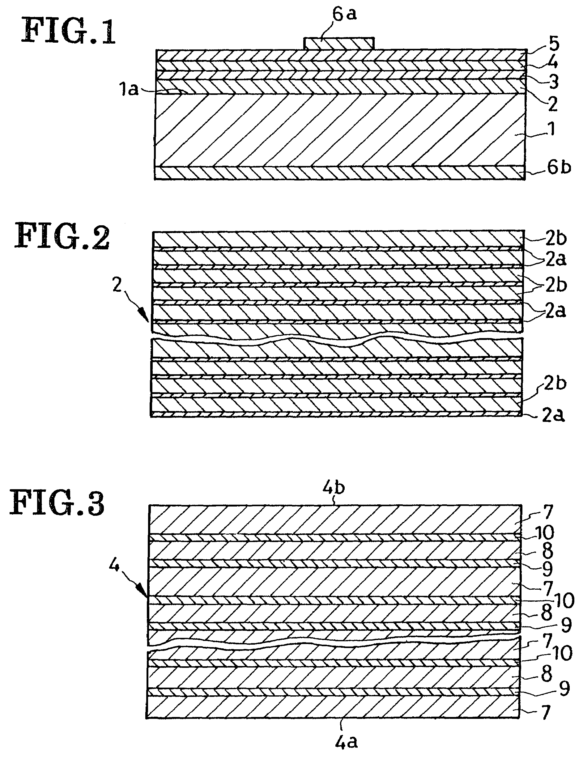
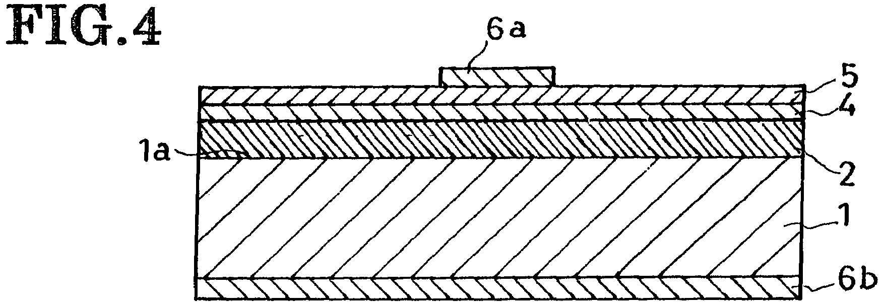
[0021]The gallium nitride light-emitting device according to the invention will now be described more specifically in terms of the light-emitting diode (LED) shown in FIG. 1. The method of fabricating this LED will be presented following the detailed explanation of its construction.

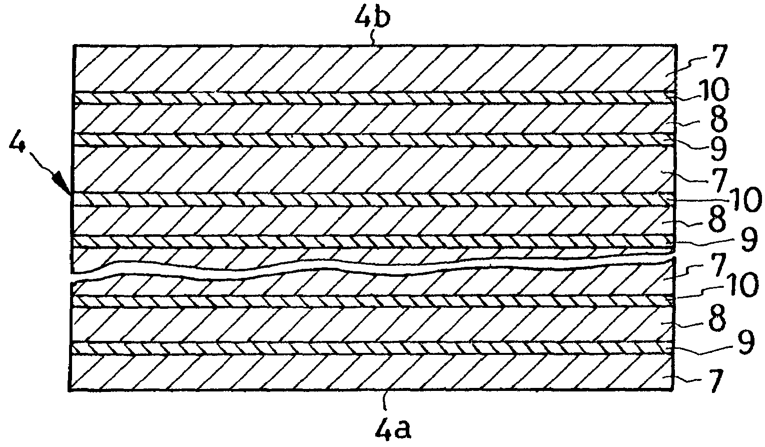
[0022]The illustrated LED has a low-resistivity substrate 1 of impurity-doped monocrystalline silicon. Formed on this substrate 1 is, first of all, an n-type buffer layer 2 shown in detail in FIG. 2, to which reference will be had presently. The buffer layer 2 is overlain by three main semiconductor layers 3, 4 and 5, which are arranged one on top of another in that order from the lowermost one upward. The lowermost main semiconductor layer 3 is an n-type cladding or confining layer; the intermediate semiconductor layer 4 is an active layer; and the topmost main semiconductor layer 5 is a p-type cladding or confining layer. The buffer layer 2 might be considered a part of the n-type semiconductor layer. A...


PUM


Abstract

A light-emitting diode has a low-resistivity silicon substrate on which there are laminated a buffer layer, an n-type lower confining layer, an active layer of multiple quantum well configuration, and a p-type upper confining layer. The active layer is constituted of cyclic alternations of a barrier sublayer of InGaN, a first complementary sublayer of AlGaInN, a well sublayer of InGaN, and a second complementary sublayer of AlGaInN. The proportions of the noted ingredients of the active sublayers are all specified. The first and the second complementary sublayers prevent the evaporation or diffusion of indium from the neighboring sublayers.

Description

CROSS REFERENCE TO RELATED APPLICATIONS[0001]This is a continuation of Application PCT / JP2003 / 013858, filed Oct. 29, 2003, which claims priority to Japanese Patent Application No. 2002-322826 filed Nov. 6, 2002.BACKGROUND OF THE INVENTION[0002]This invention relates to light-emitting semiconductor devices such as what is called the light-emitting diode in common parlance, particularly to those employing nitrides or nitride-based compounds as semiconductors, and more particularly to an active layer of improved quantum well structure included in such light-emitting devices. The invention also pertains to a method of making such light-emitting semiconductor devices.[0003]Japanese Unexamined Patent Publication Nos. 8-264832 and 2001-313421 are hereby cited as dealing with high-intensity light-emitting nitride semiconductor devices. For production of light ranging from ultraviolet to green, these known devices have their active region made from the class of gallium nitrides that are gene...

Claims


Application Information

Patent Timeline
Patent Type & Authority Patents(United States)
IPC IPC(8): H01L29/06H01L33/00H01L33/06
CPCH01L33/06H01L33/007
Inventor OHTSUKA, KOJISATO, JUNJIMOKU, TETSUJITANAKA, YOSHITAKATAJIMA, MIKIO
Owner SANKEN ELECTRIC CO LTD
Why Eureka
Try Eureka