Light emitting device and method of driving the light emitting device

a technology of light emitting device and electric element, which is applied in the direction of static indicating device, solid-state device, instruments, etc., can solve the problem of voltage endurance of tfts structure other parts tending to become a problem, and achieve the effect of reducing the deterioration of el elements

Inactive Publication Date: 2007-02-13
SEMICON ENERGY LAB CO LTD
View PDF54 Cites 46 Cited by
  • Summary
  • Abstract
  • Description
  • Claims
  • Application Information

AI Technical Summary

Benefits of technology

[0017]An object of the present invention is to propose a specific pixel structure and driving method for cases in which SES drive is employed

Problems solved by technology

Specifically, application of a reverse bias by a conventional method is performed by changing an electric power source potential, and therefore

Method used


Image

  • Light emitting device and method of driving the light emitting device
  • Light emitting device and method of driving the light emitting device
  • Light emitting device and method of driving the light emitting device

Examples


embodiment mode 1

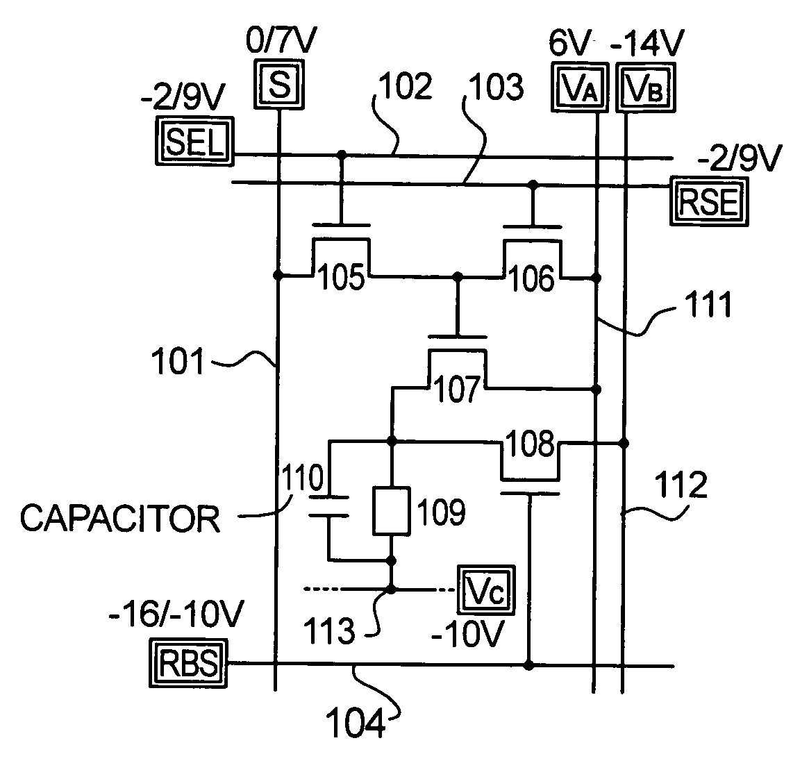
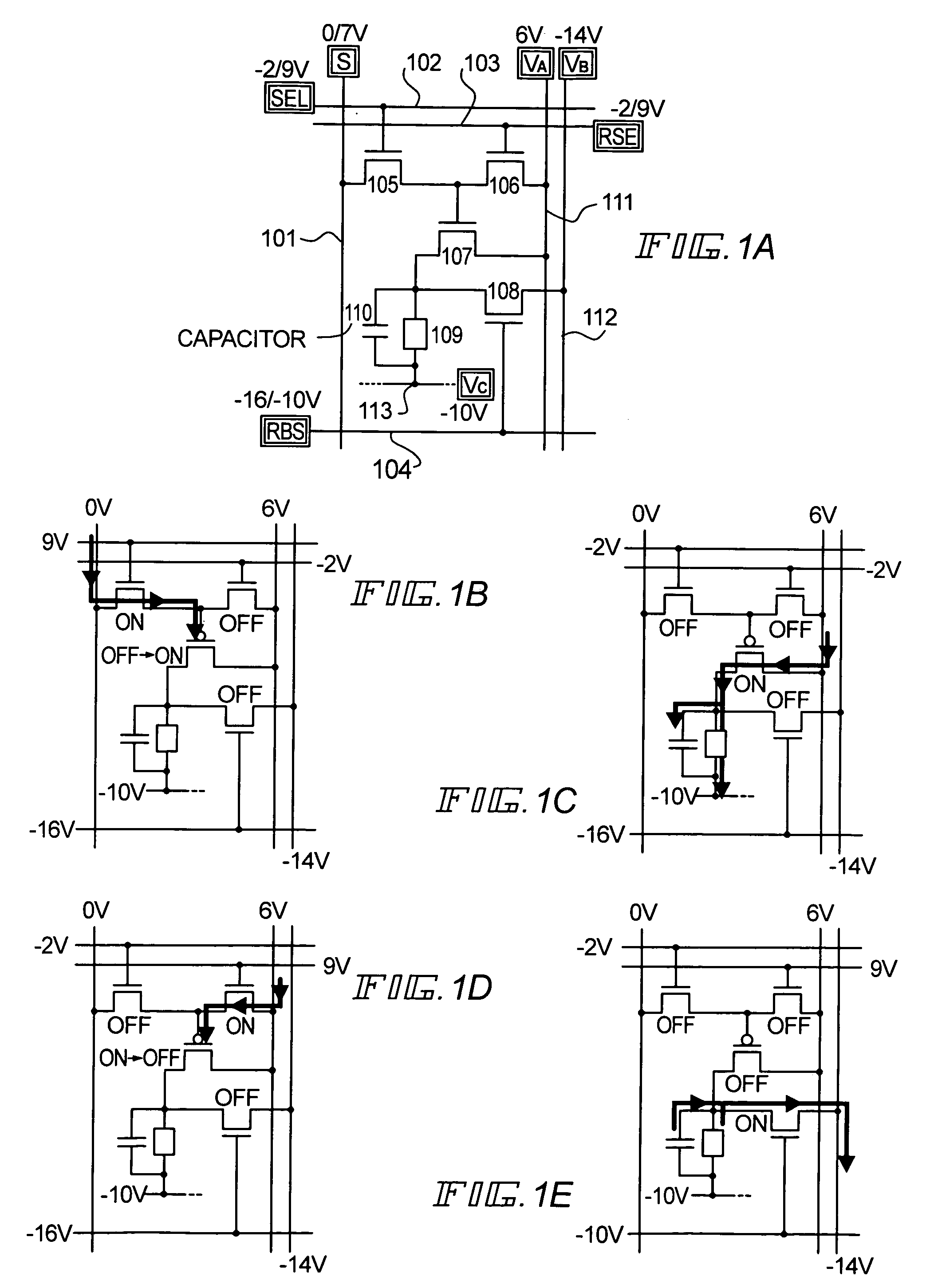
[0137]FIGS. 1A to 1E show an embodiment mode of a pixel structure for performing alternating current drive by the present invention.

[0138]As shown in FIG. 1A, each pixel has a source signal line (S) 101, a write-in gate signal line (SEL) 102, an erasure gate signal line (RSE) 103, a reverse bias gate signal line (RBS) 104, a switching TFT 105 as a third means, an erasure TFT 106 as a fifth means, a driver TFT 107 as a fourth means, a reverse bias TFT 108 as a sixth means, an EL element 109, an electric current supply line (VA) 111, and a reverse bias electric power source line (VB) 112. One electrode of the EL element 109 (pixel electrode) is connected to a source region or a drain region of the driver TFT 107, and the other electrode of the EL element 109 (opposing electrode) is connected to an opposing electric power source line (VC) 113.

[0139]Electric potentials on each signal line and electric power source line within FIG. 1A are shown as electric power source potentials, or by ...

embodiment mode 2

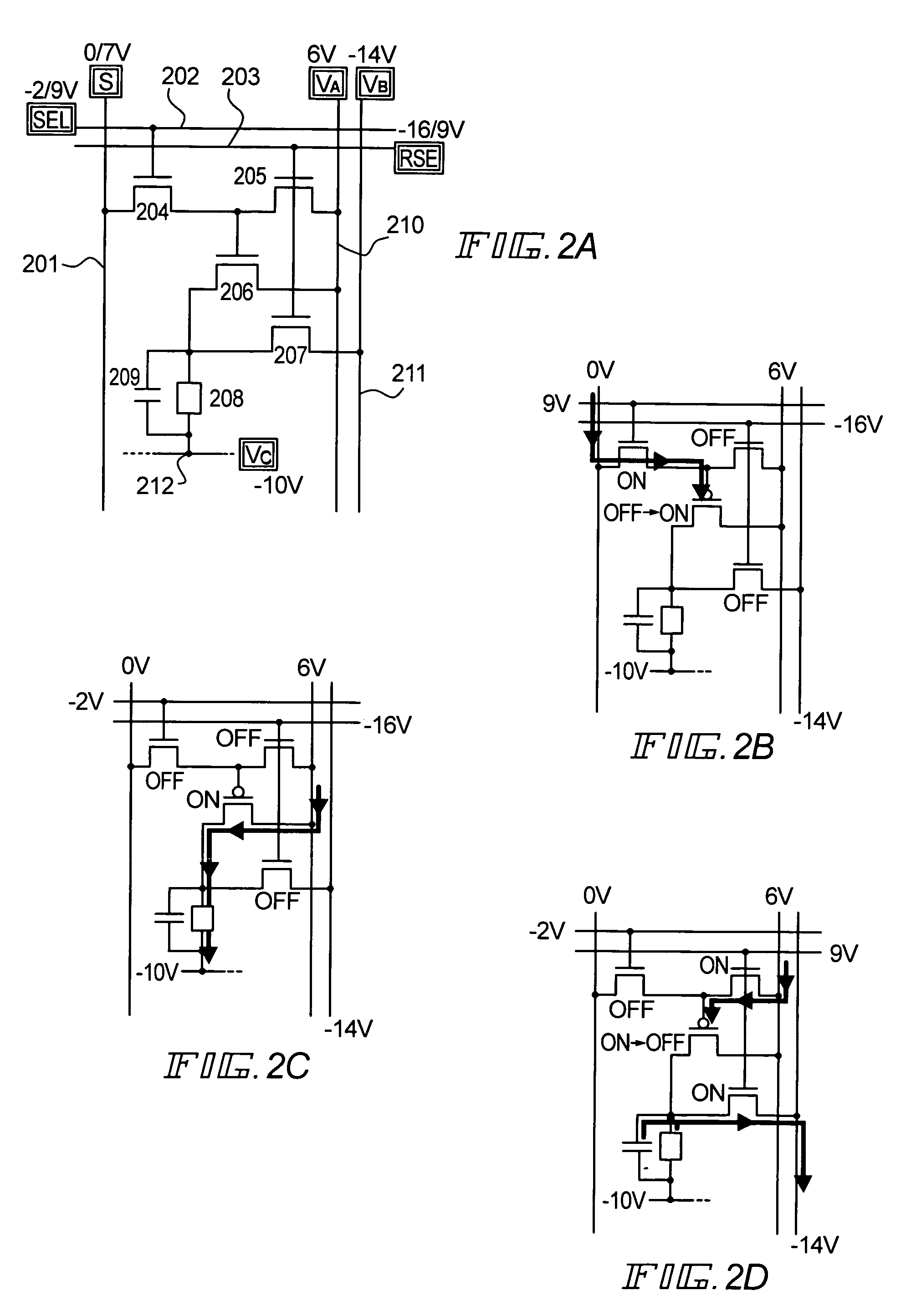
[0147]FIGS. 2A to 2D show an embodiment mode, which differs from embodiment mode 1, of a pixel structure for performing alternating current drive by the present invention.

[0148]As shown in FIG. 2A, each pixel has a source signal line (S) 201, a write-in gate signal line (SEL) 202, an erasure and reverse bias gate signal line (RSE) 203, a switching TFT 204, an erasure TFT 205, a driver TFT 206, a reverse bias TFT 207, an EL element 208, an electric current supply line (VA) 210, and a reverse bias electric power source line 211 (VB). One electrode of the EL element 208 (pixel electrode) is connected to a source region or a drain region of the driver TFT 206, and the other electrode of the EL element 208 (opposing electrode) is connected to an opposing electric power source line (VC) 212.

[0149]Electric potentials on each signal line and electric power source line within FIG. 2A are shown as electric power source potentials, or by signal L level and H level electric potentials. For exam...

embodiment mode 3

[0157]FIGS. 3A to 3E show an embodiment mode, which differs from embodiment modes 1 and 2, of a pixel structure for performing alternating current drive by the present invention.

[0158]As shown in FIG. 3A, each pixel has a source signal line (S) 301, a write-in gate signal line (SEL) 302, an erasure gate signal line (RSE) 303, a reverse bias gate signal line (RBS) 304, a switching TFT 305, a driver TFT 306, an erasure TFT 307, a reverse bias TFT 308, an EL element 309, an electric current supply line (VA) 311, and a reverse bias electric power source line (VB) 312. One electrode of the EL element 309 (pixel electrode) is connected to a source region or a drain region of the driver TFT 306 through the erasure TFT 307, and the other electrode of the EL element 309 (opposing electrode) is connected to an opposing electric power source line (VC) 313.

[0159]Electric potentials on each signal line and electric power source line within FIG. 3A are shown as electric power source potentials, o...


PUM


Abstract

A light emitting device that achieves long life, and which is capable of performing high duty drive, by suppressing initial light emitting element deterioration is provided. Reverse bias application to an EL element (109) is performed one row at a time by forming a reverse bias electric power source line (112) and a reverse bias TFT (108). Reverse bias application can therefore be performed in synchronous with operations for write-in of an image signal, light emission, erasure, and the like. Reverse bias application therefore becomes possible while maintaining a duty equivalent to that of a conventional driving method.

Description

BACKGROUND OF THE INVENTION[0001]1. Field of the Invention[0002]The present invention relates to an electroluminescence (EL) element, and a method of driving a light emitting device manufactured by forming thin-film transistors (hereinafter abbreviated as TFTs) on a substrate. Particularly, the present invention relates to an electronic apparatus which uses the light emitting device as display units. Here, as a typical example of light emitting elements, the EL elements will be described.[0003]In this specification, the EL elements include the ones which utilize emission of light from singlet excitons (fluorescence) and the ones which utilize the emission of light from triplet excitons (phosphorescence).[0004]2. Description of the Related Art[0005]In recent years, light-emitting devices having EL elements as the light emitting elements have been vigorously developed as light emitting elements. Unlike liquid crystal display devices, the light-emitting device is of self emission type....

Claims


Application Information

Patent Timeline
IPC IPC(8): G09G3/30G09G3/10H01L51/50G09G3/20
CPCG09G3/3258G09G3/3233H01L33/0041G09G3/3266G09G3/3291G09G2300/043G09G2300/0842G09G2300/0861G09G2310/0256G09G2310/027G09G2310/061G09G2320/043G09G2310/0251G09G2310/08G09G3/32G09G2300/0819G09G2320/045
Inventor OSAME, MITSUAKIANZAI, AYATANADA, YOSHIFUMIMIYAGAWA, KEISUKESEO, SATOSHIYAMAZAKI, SHUNPEI
Owner SEMICON ENERGY LAB CO LTD
Why Eureka
Try Eureka