Wafer processing method

a processing method and resin film technology, applied in the field of laser processing methods, can solve the problems of deteriorating semiconductor chips, affecting the processing efficiency of laser beams, and affecting the processing efficiency of laser beams, and achieve the effect of suppressing the partial peeling of resin films

Active Publication Date: 2007-02-20
DISCO CORP
View PDF6 Cites 139 Cited by
  • Summary
  • Abstract
  • Description
  • Claims
  • Application Information

AI Technical Summary

Benefits of technology

[0009]It is an object of the present invention to provide a wafer processing method capable of preventing the influence of debris produced by applying a laser beam to a wafer.
[0017]Since in the laser processing method of the present invention, the resin film that absorbs a laser beam is formed on the surface to be processed of the wafer and then, the laser beam is applied to the wafer through the resin film, the resin film absorbing the laser beam becomes a processing start point. Since the wafer is processed by the application of the laser beam after the processing start point is formed in the resin film, the generation of impact force caused by the laser beam passing through the resin film can be prevented, thereby suppressing the partial peeling of the resin film. Therefore, it is possible to prevent debris from adhering to the outer periphery of the chip exposed by the partial peeling of the resin film.

Problems solved by technology

When the above semiconductor wafer having a Low-k film laminated thereon is cut along the streets with the cutting blade, there is a problem that as the Low-k film is extremely fragile like mica, the Low-k film peels off, and this peeling reaches the circuits and causes a fatal damage to the semiconductor chips.
Even in a semiconductor wafer having no Low-k film, when the film laminated on the front surface of the semiconductor substrate is cut along the streets with the cutting blade, a problem occurs that it peels off by destructive force generated by the cutting operation of the cutting blade, thereby damaging the semiconductor chips.
When a laser beam is applied along the streets of the semiconductor wafer, however, heat energy is concentrated on the area to which the laser beam has been applied to produce debris which adhere to a bonding pad connected to a circuit, thereby deteriorating the semiconductor chip.
When the surface to be processed of the workpiece is covered with the protective film and a laser beam is applied to the workpiece through the protective film, however, the laser beam passes through the protective film to process the workpiece and its impact force peels off part of the protective film to cause debris to adhere to the outer periphery of the exposed chip.

Method used


Image

  • Wafer processing method
  • Wafer processing method
  • Wafer processing method

Examples


Embodiment Construction

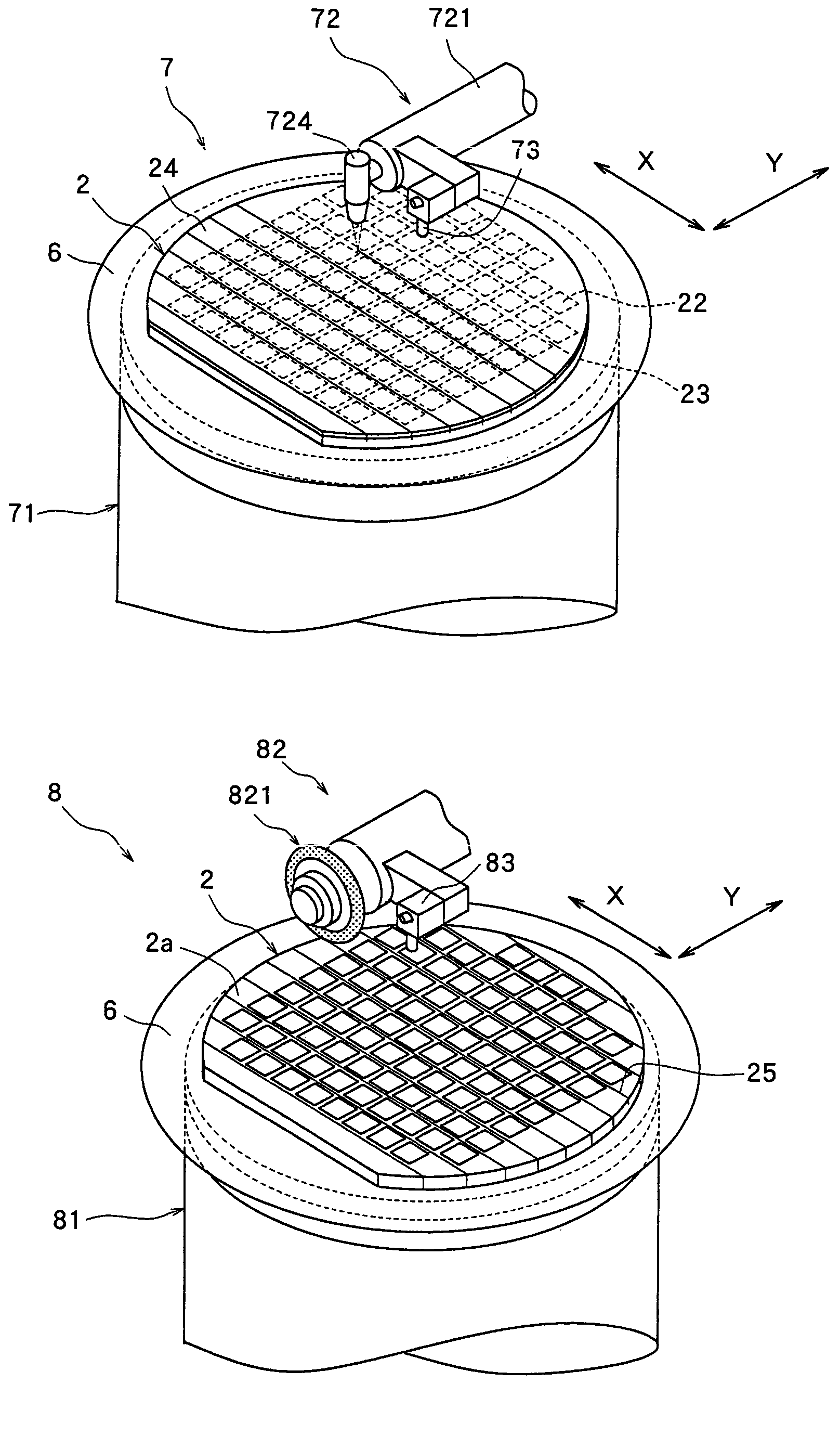
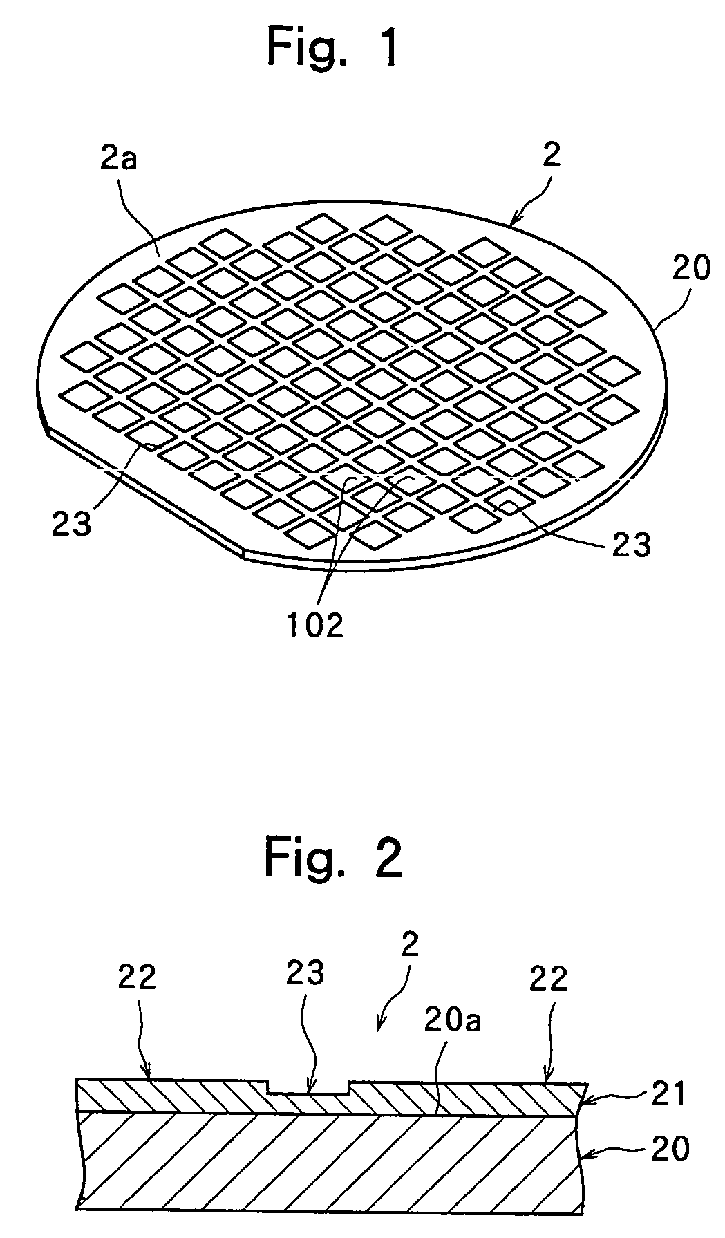
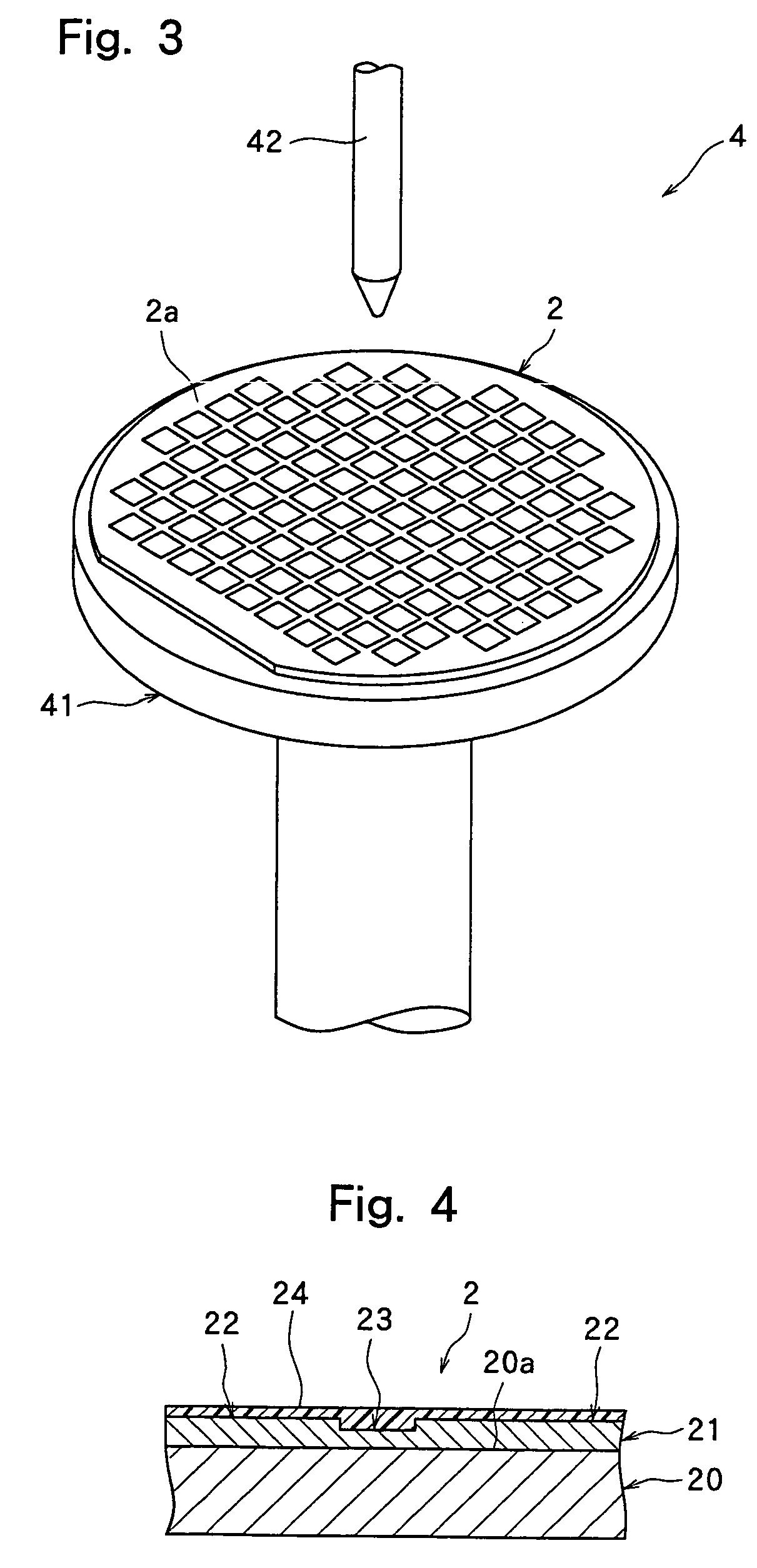
[0041]The wafer processing method of the present invention will be described in more detail with reference to the accompanying drawings.

[0042]FIG. 1 is a perspective view of a semiconductor wafer as a workpiece to be processed by the wafer processing method of the present invention and FIG. 2 is an enlarged sectional view of the principal section of the semiconductor wafer shown in FIG. 1. In the semiconductor wafer 2 shown in FIG. 1 and FIG. 2, a plurality of semiconductor chips 22 such as IC's or LSI's, which are composed of a laminate 21 consisting of an insulating film and a functional film forming circuits and formed in a matrix on the front surface 20a of a semiconductor substrate 20 such as a silicon substrate. The semiconductor chips 22 are sectioned by streets 23 formed in a lattice pattern. In the illustrated embodiment, the insulating film forming the laminate 21 is an SiO2 film or a low-dielectric insulating film (Low-k film) formed of a film of an inorganic material suc...


PUM

PropertyMeasurementUnit
wavelengthaaaaaaaaaa
diameteraaaaaaaaaa
diameteraaaaaaaaaa

Abstract

A laser beam processing method for processing a wafer by applying a laser beam to a predetermined area, comprising the steps of forming a resin film which absorbs a laser beam, on the surface to be processed of the wafer; applying a laser beam to the surface to be processed of the wafer through the resin film; and removing the resin film after the laser beam application step.

Description

FIELD OF THE INVENTION[0001]The present invention relates to a laser processing method for carrying out predetermined processing by applying a laser beam to a predetermined area of a wafer such as a semiconductor wafer or an optical device wafer.DESCRIPTION OF THE PRIOR ART[0002]As is known to people of ordinary skill in the art, a semiconductor wafer comprising a plurality of semiconductor chips such as IC's or LSI'S, which are composed of a laminate consisting of an insulating film and a functional film and formed in a matrix on the front surface of a semiconductor substrate such as a silicon substrate is manufactured in the production process of a semiconductor device. The above semiconductor chips are sectioned by dividing lines called “streets” in this semiconductor wafer and separated from one another by cutting the semiconductor wafer along the streets. An optical device wafer comprising optical devices composed of gallium nitride-based compound semiconductors laminated in a ...

Claims


Application Information

Patent Timeline
Patent Type & Authority Patents(United States)
IPC IPC(8): H01L21/301B23K26/18B23K26/38B23K26/40B23K101/40H01L21/00H01L21/44H01L21/78
CPCB23K26/18H01L21/78B23K26/367H01L21/67092B23K26/364
Inventor GENDA, SATOSHIYOSHIKAWA, TOSHIYUKIOBA, RYUGOFURUTA, KENJIKITAHARA, NOBUYASU
Owner DISCO CORP
Why Eureka
Try Eureka