
Organic electro luminescent display panel and fabricating method thereof

a luminescent display panel and organic technology, applied in the field of organic electro luminescent (el) display panels, can solve the problems of reducing the aperture ratio of the pixel, the inability to uniformly brighten the organic el display panel, and the relatively long time it takes to charge the parasite capacitor of the data line, etc., to achieve the effect of improving the arrangement structure of the unit pixel and increasing the aperture ratio

Active Publication Date: 2007-02-27
SAMSUNG DISPLAY CO LTD
View PDF4 Cites 18 Cited by
  • Summary
  • Abstract
  • Description
  • Claims
  • Application Information

AI Technical Summary

Benefits of technology

The present invention provides an organic EL display panel with an increased aperture ratio by improving the arrangement structure of a unit pixel. The panel includes at least one pixel circuit with an organic light emitting element, thin film transistors, and a capacitor per pixel. The method for fabricating the panel includes forming a common semiconductor layer for at least two thin film transistors, adding a gate insulation film, forming gate electrodes, adding an interlayer insulation film, and forming a conductive layer inside a contact hole. The technical effect of the invention is to increase the aperture ratio of the display panel, resulting in improved image quality.

Problems solved by technology

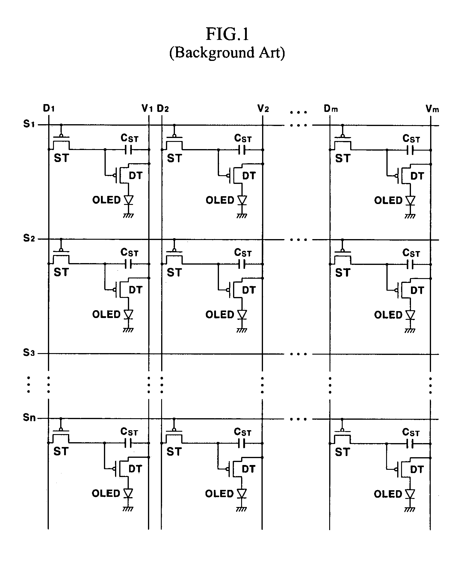
In the voltage programming method as described above, a problem may arise in that brightness of an organic EL display panel may not be uniform due to deviation in characteristics of driving thin film transistors, such as threshold voltage or channel mobility.
However, increasing the number of thin film transistors may decrease the pixel's aperture ratio.
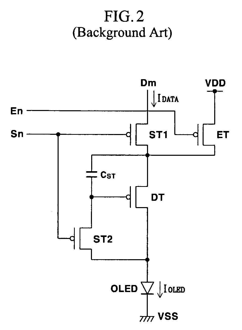
However, since the current IOLED flowing through the organic light emitting element OLED may be minute, and the voltage range of the data line Dm may be wide, it may take a relatively long time to charge a parasite capacitor of the data line.
Additionally, increasing the number of thin film transistors disposed in a unit pixel may significantly reduce the aperture ratio, which may deteriorate brightness.

Method used


Image

  • Organic electro luminescent display panel and fabricating method thereof
  • Organic electro luminescent display panel and fabricating method thereof
  • Organic electro luminescent display panel and fabricating method thereof

Examples


Embodiment Construction

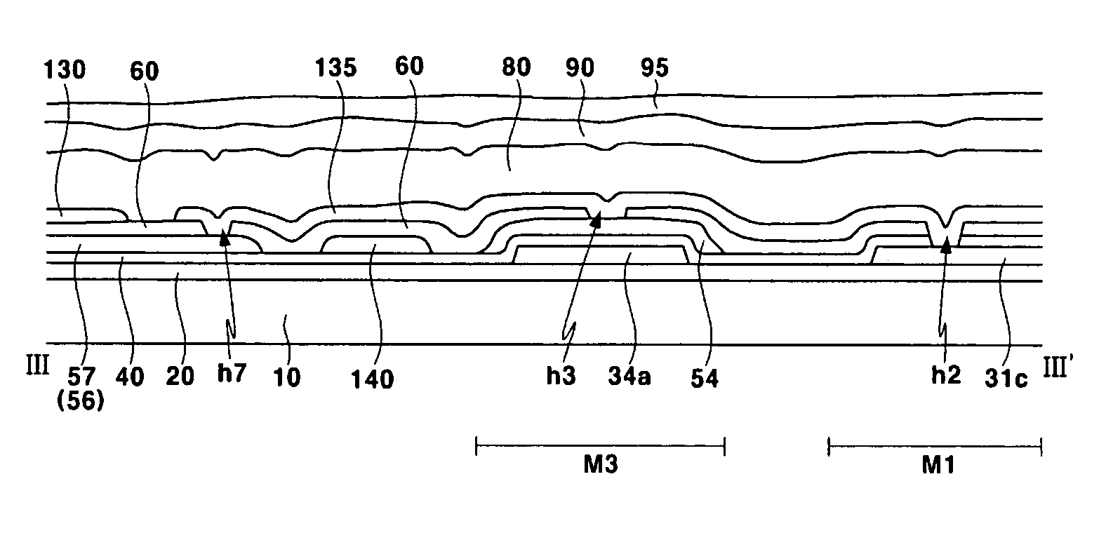
[0032]The following detailed description shows and describes exemplary embodiments of the present invention. As those skilled in the art would recognize, the described exemplary embodiments may be modified in various ways, all without departing from the spirit or scope of the present invention.

[0033]In the drawings, illustrations of elements having no relation with the present invention are omitted in order to prevent the subject matter of the present invention from being unclear. In the specification, the same or similar elements are denoted by the same reference numerals even though they are depicted in different drawings. As used herein, a coupling between one element and another element includes not only a direct coupling therebetween but also an indirect coupling therebetween with other elements interposed therebetween. In addition, forming one element such as a layer, a film, a region or a plate on another element includes not only forming the former immediately above the latt...


PUM


Abstract

There is provided an organic EL display panel having a pixel circuit that increases the panel's aperture ratio by an improved structure of a unit pixel. The present invention discloses an organic EL display panel including at least one pixel circuit for driving each pixel, wherein the pixel circuit comprises at least one organic light emitting element, at least two thin film transistors and at least one capacitor per pixel. The thin film transistors respectively comprise a gate electrode and a semiconductor layer in which a channel region, a source region and a drain region are formed. The conductive layer contacted on the gate electrode of one of the thin film transistors is coupled to another thin film transistor and at least one capacitor.

Description

CROSS REFERENCE TO RELATED APPLICATION[0001]This application claims priority to and the benefit of Korean Patent Application No. 10-2004-0037278, filed on May 25, 2004, which is hereby incorporated by reference for all purposes as if fully set forth herein.BACKGROUND OF THE INVENTION[0002]1. Field of the Invention[0003]The present invention relates to an organic electro luminescent (EL) display panel, and more particularly to an organic EL display panel in which an aperture ratio is increased by improving a structure of a unit pixel.[0004]2. Description of the Background[0005]An organic EL display uses light emitted from an electrically excited organic light emitting diode OLED to display characters or images. Electrons, supplied from a cathode, and holes, supplied from an anode, recombine to excite the organic material. Generally, the organic light emitting diode OLED includes an anode electrode layer, an emitting layer (EML) for facilitating supply of electrons and holes, an elect...

Claims


Application Information

Patent Timeline
Patent Type & Authority Patents(United States)
IPC IPC(8): G09G3/30G09F9/30G09G3/10H05B33/10G09G3/32G09G3/36H01L21/77H01L27/12H01L27/13H01L27/32H01L51/50H05B33/14H05B44/00
CPCG09G3/325H01L27/1255G09G3/3655G09G2300/0852H01L27/124G09G2320/0223H01L27/3244G09G2300/0861H10K59/12G09G3/3233H10K59/1213H10K59/131
Inventor KIM, KEUM-NAM
Owner SAMSUNG DISPLAY CO LTD
Learn More