Supercharge Your Innovation With Domain-Expert AI Agents!

Memory circuit and method for processing a code to be loaded into a memory circuit

a memory circuit and code technology, applied in the field of memory circuits, can solve the problems of increasing the capacity of roms, serious problems for development teams, and memory testing with traditional tools available to engineers, and achieve the effect of easy testing

Active Publication Date: 2007-02-27
STMICROELECTRONICS SRL
View PDF6 Cites 2 Cited by
  • Summary
  • Abstract
  • Description
  • Claims
  • Application Information

AI Technical Summary

Benefits of technology

"The present invention provides a read-only memory structure that remains easy to test even when the number of cells within the matrix increases. It also allows integration of the memory structure within an integrated circuit and improves the gradient of vias within the memory structure. The memory structure has a constant access time regardless of the bit line considered. The invention also includes a method for checking groups of memory cells sequentially with each group being associated with one of multiplexers. The technical effects of the invention include improved performance and reduced transit times."

Problems solved by technology

However, increasing the capacity of ROMs poses serious problems for development teams.
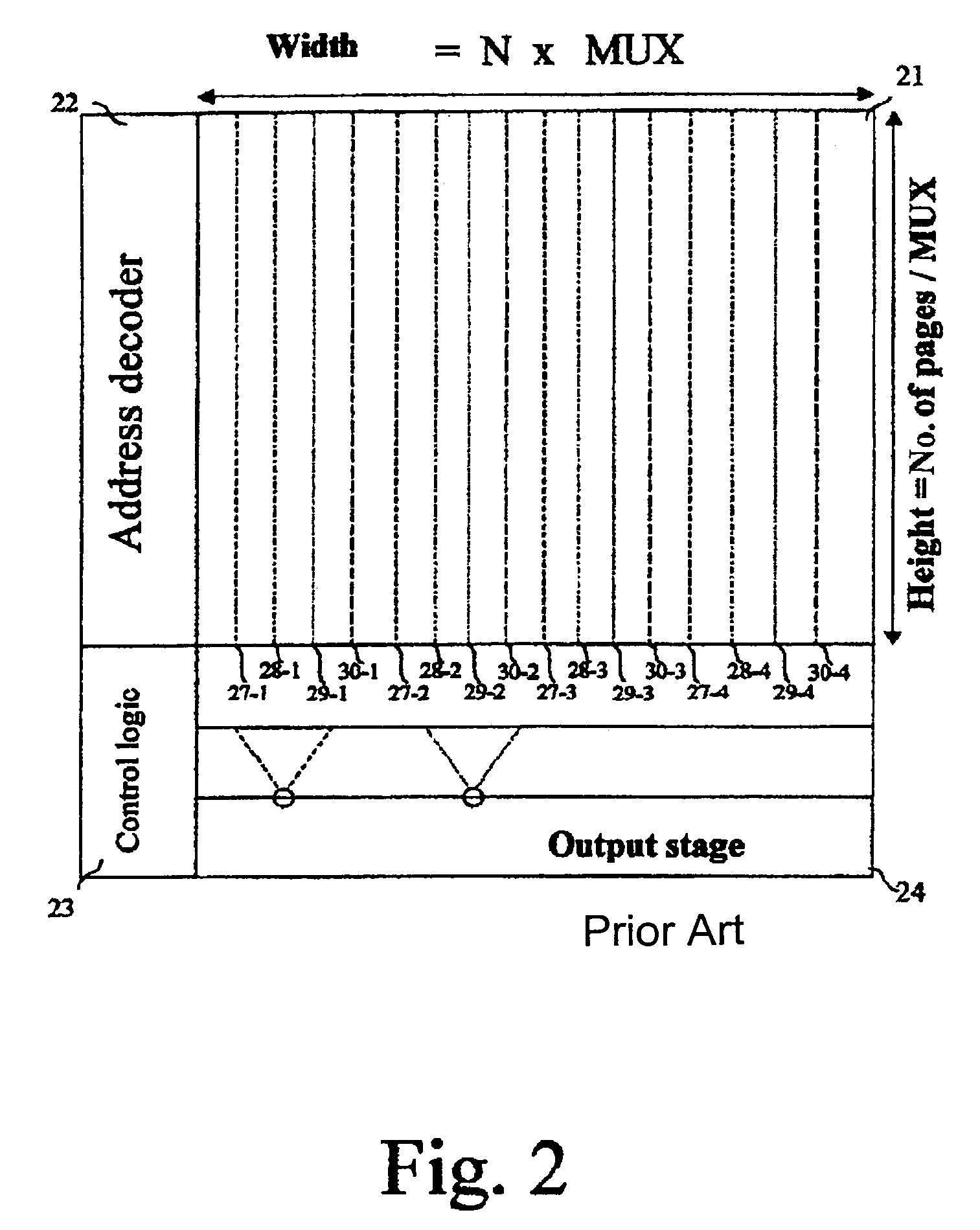
For example, a first problem results from the increase in memory size that can currently reach 8, 16 or even 32 megabits, which makes memories extremely difficult to test with the traditional checking tools available to engineers.
It is, however, not satisfactory.
Indeed, it tends to create a considerable tangle among the columns forming the matrix network and, consequently, makes checking thereof very difficult.
Traditional checking techniques and systems, in particular the ones based on Layout Versus Schematics (LVS), very quickly prove unable to run low level testing on a ROM of such size.
This amounts to coding and processing a file or database containing several million bytes, which greatly exceeds the capacities of conventional checking devices.
Thus, it is then necessary to invest in newer, more powerful and more expensive check and test tools that will in turn become obsolete and insufficient when the size of ROM increases again.
To this major difficulty is added a second problem that results from the fact that the storage of some programs can lead to a great disparity of pattern densities, thus leading to important gradients within the matrix.
Such occurrence of gradients proves to be cumbersome especially with the increasing miniaturization of patterns and it is desirable to be able to reduce the value of these gradients.
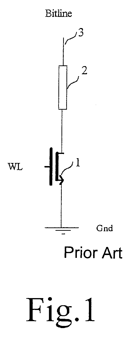
Furthermore, the presence of inverters in some bit lines introduces a third problem linked to the considerable access time within the memory, which also needs to be reduced.

Method used


Image

  • Memory circuit and method for processing a code to be loaded into a memory circuit
  • Memory circuit and method for processing a code to be loaded into a memory circuit
  • Memory circuit and method for processing a code to be loaded into a memory circuit

Examples


Embodiment Construction

[0036]Preferred embodiments of the present invention will be described in detail hereinbelow with reference to the attached drawings.

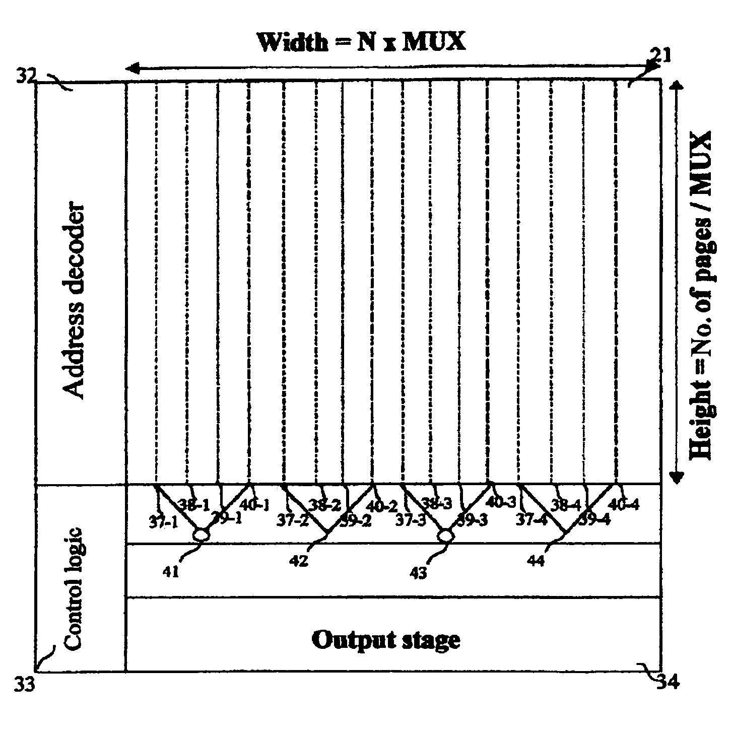
[0037]FIG. 3 illustrates a preferred embodiment of the present invention. There is shown a structure of a read-only memory in matrix form, which is made up of a number of rows forming as many pages, with each page consisting of four words of four bits each. These values are not meant to be limiting but have been selected for the sake of simplification only, and those skilled in the art can easily adapt the structure to any memory characteristic.

[0038]The memory comprises a matrix 31 organized in rows (WORDLINE) and columns (BITLINE) like a traditional ROM memory.

[0039]Generally, when designing an on board memory, such memory is defined by the number of rows it comprises, corresponding to the number of pages that can be accessed, by a multiplexing rate (MUX), corresponding to the number of words contained in each page, and by a number of bits, N, for ea...


PUM


Abstract

A ROM-type memory is provided that includes a matrix of memory cells made up of rows and columns, with each row allowing storage of a page of MUX words of N bits. An address decoder decodes addresses in order to extract the page to be read. At the output of the matrix, N multiplexers are each coupled to the columns that correspond to one of the bits of the output stage. An N-bit output stage includes at least one inverter, with each of the inverters being connected to the output of one of the multiplexers so as to restore inverted values of information to be stored to correct values. The inverted values are stored in all of the memory cells of all of the columns coupled to the one multiplexer. Storing the inverted values makes it possible to store less “0” values within the matrix and further makes LVS testing of the ROM memory considerably easier. Also provided is a method for sequentially checking groups of memory cells.

Description

CROSS-REFERENCE TO RELATED APPLICATIONS[0001]This application is based upon and claims priority from French Patent Application No. 03 13354, filed Nov. 14, 2003, the entire disclosure of which is herein incorporated by reference.FIELD OF THE INVENTION[0002]The present invention relates to memory circuits, and in particular to a ROM-type memory circuit comprising a matrix of memory cells having rows and columns, with each row allowing storage of a page of MUX words of N bits.BACKGROUND OF THE INVENTION[0003]More and more electronic devices are equipped with semiconductor products including a microcomputer associated with an on board memory on the same semiconductor product, thus making up a real system on chip.[0004]Increasing the power of such systems is done in particular by increasing the capacity of the Read Only Memories (ROM) that are used for storing the microprograms required to operate the integrated microcomputer.[0005]However, increasing the capacity of ROMs poses serious ...

Claims


Application Information

Patent Timeline
Patent Type & Authority Patents(United States)
IPC IPC(8): G11C17/00G11C29/00G11C7/00G11C7/10G11C17/10G11C17/14
CPCG11C17/14G11C17/10
Inventor TURGIS, DAVID
Owner STMICROELECTRONICS SRL
Features
  • R&D
  • Intellectual Property
  • Life Sciences
  • Materials
  • Tech Scout
  • Unparalleled Data Quality
  • Higher Quality Content
  • 60% Fewer Hallucinations
Learn More