Semiconductor memory device

a technology of memory device and semiconductor, which is applied in the direction of information storage, static storage, digital storage, etc., can solve the problems of inability to re-enter the data retention mode of super low power consumption, and the system cannot make re-entry immediately into the data retention mode, so as to improve the system performance and improve the system performance

Inactive Publication Date: 2007-02-27
LONGITUDE LICENSING LTD
View PDF6 Cites 53 Cited by
  • Summary
  • Abstract
  • Description
  • Claims
  • Application Information

AI Technical Summary

Benefits of technology

[0059]Accordingly it is an object of the present invention to provide a semiconductor memory device in which the system may re-enter into the data retention mode of super low power consumption without standby to enable other operations, and a controlling method therefor.
[0060]Another object of the present invention is to provide a semiconductor memory device in which reversion may be made quickly to the idle state at the time of exiting from the data retention mode of the super low power consumption, and a controlling method therefor.
[0077]Moreover, according to the present invention, return to the idle state may be made promptly, when exiting from the data retention mode with low power consumption, thus contributing to improvement in the system performance. In addition, according to the present invention, re-entry may be made during the operation of exiting from the data retention operating mode with low power consumption, thus further contributing to improvement of system performance.

Problems solved by technology

That is, in case the semiconductor memory device has commenced the operation of exiting from the data retention mode of super low power consumption, as a result of issuing the command for entry into the data retention mode of super low power consumption, it is not possible for the system to make re-entry immediately into the data retention mode of super low power consumption to proceed to the next processing.
That is, re-entry to the data retention mode of the super low power consumption is not possible until after the end of the sequence of the above operations.

Method used


Image

  • Semiconductor memory device
  • Semiconductor memory device
  • Semiconductor memory device

Examples


Embodiment Construction

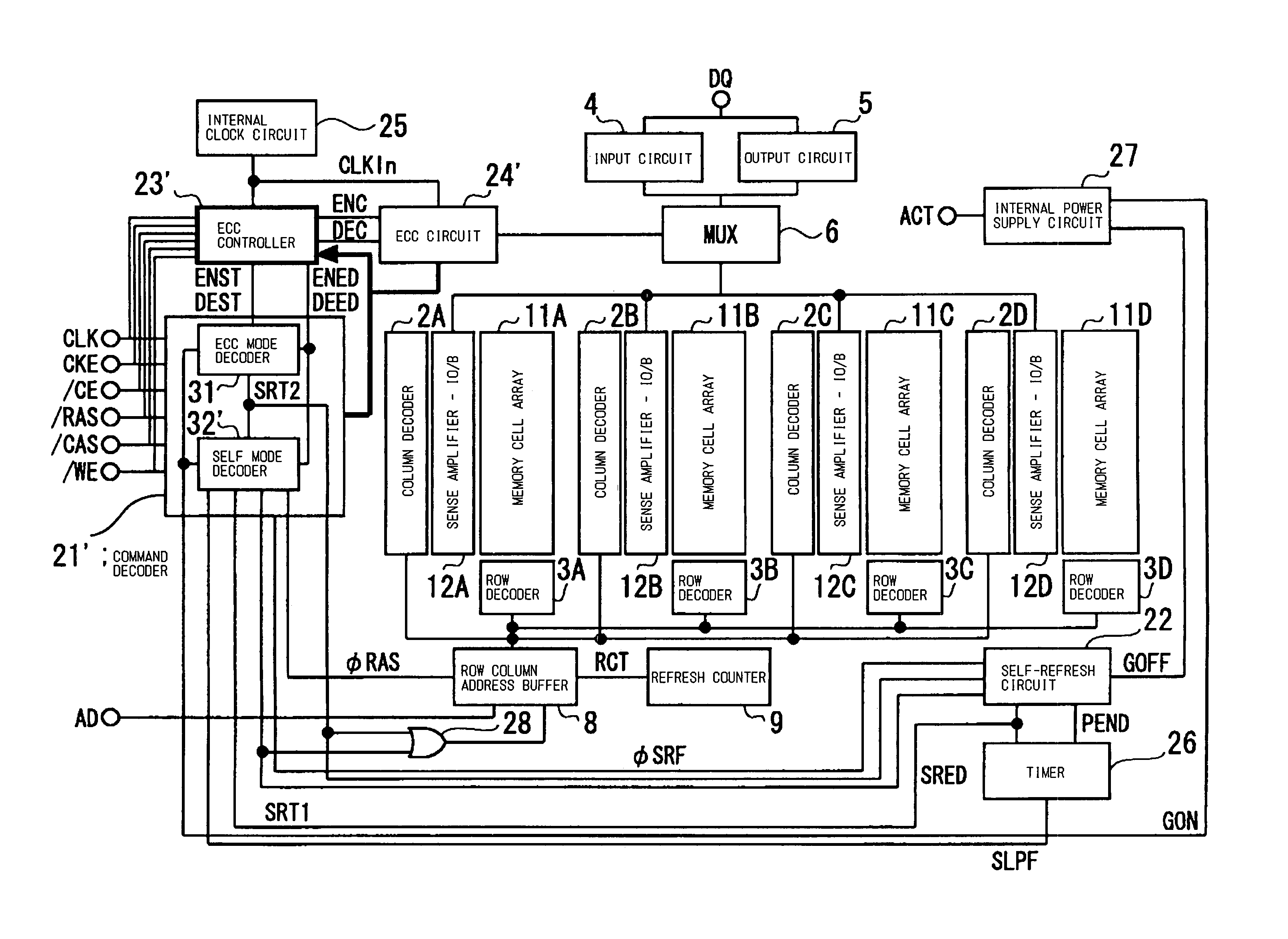
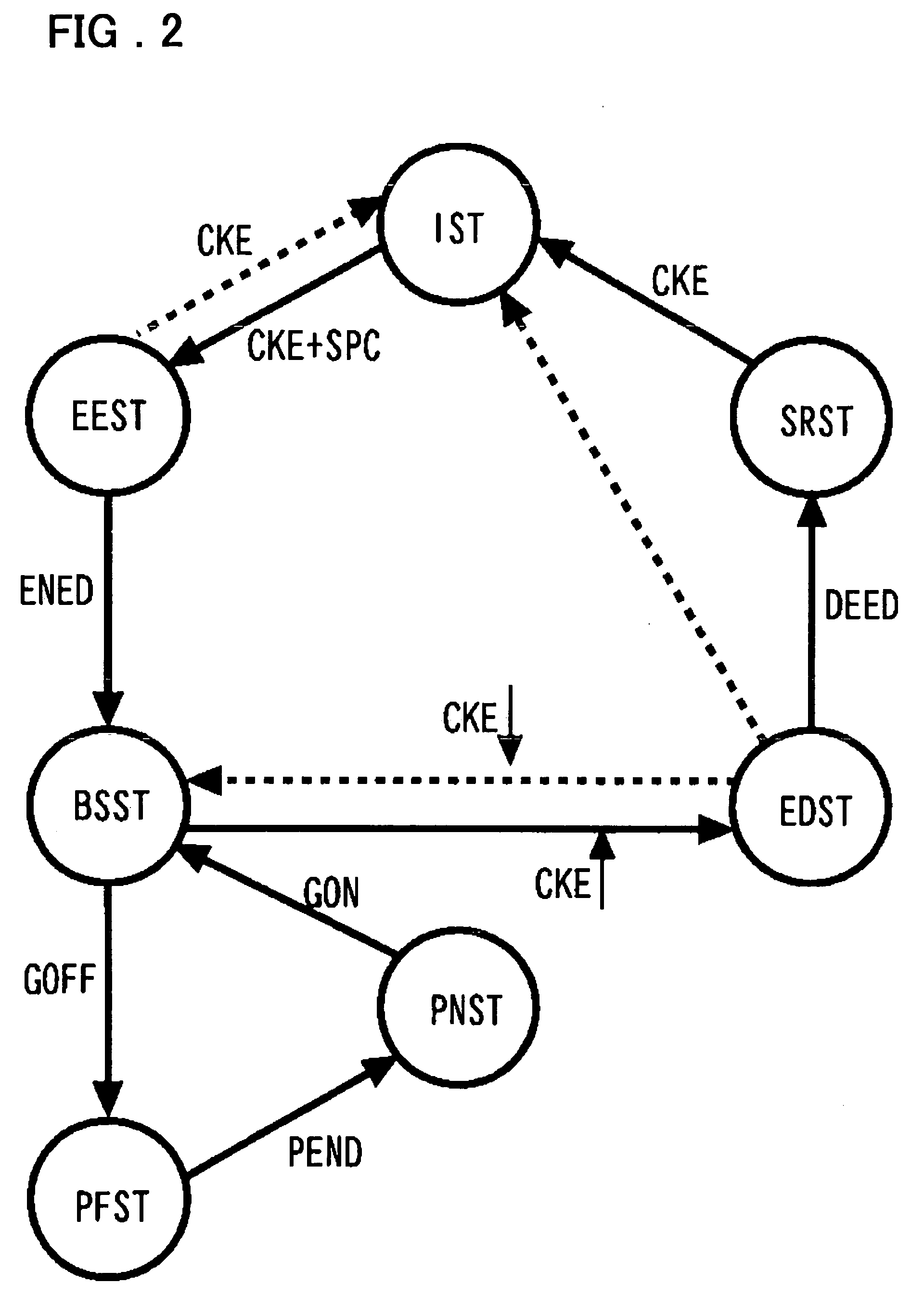
[0091]The preferred embodiments of the present invention will now be described. With a semiconductor memory device according to the present invention, the status transition, shown in FIG. 12, has been improved, and the use of a DRAM device which includes an on-chip ECC circuit and has the function of the data retention mode of the super low power consumption, as described in connection with FIGS. 11 and 12, is presupposed. That is, the present invention is premised on the use of a DRAM device including an on-chip ECC (error correction circuit) and having, as the data retention mode (standby state), such a mode in which the parity information is generated by the ECC circuit and written in a check bit area of the memory cell array, cell refresh is carried out in a burst, at least part of the internal power supply circuit is turned off by way of power control, and in which the refresh failure cells are corrected for errors in the ECC circuit to elongate the refresh period to reduce the...


PUM


Abstract

A semiconductor memory device including an on-chip ECC circuit and having a data retention mode which includes, in the order of state transition, an encoding state EEST by an error correction circuit in which the error correction circuit carries out calculation of parity bits of data of the memory cells, a burst self-refresh state BSST in which the memory cells are self-refreshed in a burst with a period shorter than in ordinary self-refresh, a power-off state PFST in which an internal power supply circuit is partially turned off, a power-on state PNST in which the internal power supply circuit, partially turned off, is turned on, and a decoding state EDST by the error correction circuit in which the error correction circuit corrects errors of the memory cells. In case a command for exiting from the data retention mode in the encoding state, transition may be made to an idle state IST so that re-entry may be made from the decoding state EDST to the BSST.

Description

FIELD OF THE INVENTION[0001]This invention relates to a power controlling method for a semiconductor memory device having memory cells in need of refresh for data retention, and a semiconductor memory device employing the power controlling method.BACKGROUND OF THE INVENTION[0002]FIG. 11 is a diagram showing the configuration of a conventional semiconductor memory device including an ECC (error checking and correction) codec (coder / decoder circuit). FIG. 11 is based on FIG. 1 of Patent Publication 1 and forms the premises of the present invention, and hence is now described schematically.[0003]Referring to FIG. 11, this semiconductor memory device is a clock synchronized type SDRAM (synchronous dynamic random access memory) including four memory cell arrays 11A to 11D in association with four memory banks. Each of the memory cell arrays 11A to 11D includes a matrix array of dynamic memory cells. The gate terminal of a memory cell transistor, not shown, is connected to a word line, no...

Claims


Application Information

Patent Timeline
Patent Type & Authority Patents(United States)
IPC IPC(8): G11C7/00G11C11/406
CPCG11C11/406G11C2211/4067G11C2211/4062
Inventor ITO, YUTAKAHASHIMOTO, TAKESHIYAMASAKI, EIJITAKEUCHI, SHIGEOKANEDA, MASAYUKI
Owner LONGITUDE LICENSING LTD
Why Eureka
Try Eureka