
Testing implementation suitable for built-in self-repair (BISR) memories

a technology of built-in self-repair and memory, applied in the direction of instruments, mechanical equipment, operating means/releasing devices of valves, etc., can solve the problems of high manufacturing difficulty, large test development cost, and high production cos

Inactive Publication Date: 2007-02-27
AVAGO TECH INT SALES PTE LTD
View PDF7 Cites 8 Cited by
  • Summary
  • Abstract
  • Description
  • Claims
  • Application Information

AI Technical Summary

Problems solved by technology

Because of the increasing complexity of new designs, test development costs can account for a large percentage of the total ASIC development cost.
This testing is necessary because perfect yields are difficult to achieve.
It is not uncommon for a certain percentage of unpackaged ASIC die to contain memory cells which fail testing processes, due largely to non-systemic manufacturing defects and degradation faults.
Such manufacturing issues are likely to increase as process geometries continue to shrink and the density of memory cells increases.
There are often problems in capturing repair information by testers based upon how the error capture mode of the tester is set up.
In some testers, when a functional error is observed, the tester starts over and incrementally captures the errors.
If the registers of all the BISR memories are connected into one scan chain (i.e., connected serially), the error capture of the test device results in incorrect information being scanned out.
This limitation does not allow the flare registers to be connected serially.
This approach, however, is unacceptable since it increases the BISR gate count by nearly 15%.
Another alternative is to use parallel loading of the output register; however, this can cause routing congestion if there are many BISR memories in the design.

Method used


Image

  • Testing implementation suitable for built-in self-repair (BISR) memories
  • Testing implementation suitable for built-in self-repair (BISR) memories
  • Testing implementation suitable for built-in self-repair (BISR) memories

Examples


Embodiment Construction

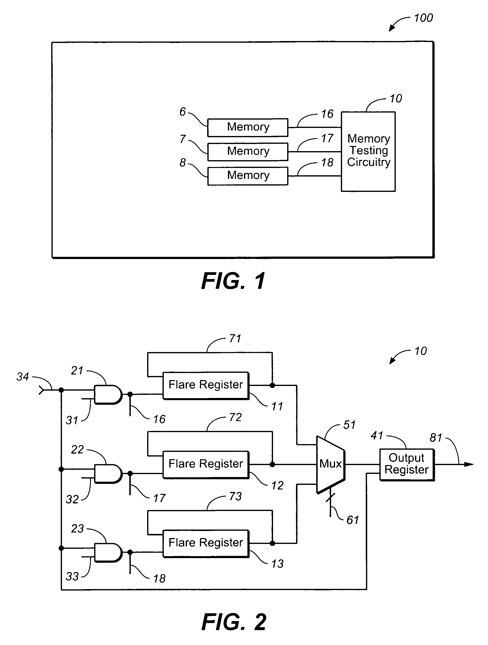
[0015]Referring now to the drawings and, more particularly to FIG. 1, a schematic diagram of an integrated circuit including memory testing circuitry constructed according to principles of the present invention is shown. In FIG. 1, an integrated circuit 100 such as an ASIC includes one or more memories with BISR logic. For purposes of explanation and example, FIG. 1 shows three memories with BISR logic represented by reference characters 6, 7 and 8. It should be intuitive, however, that any number of such BISR memories may be included on the integrated circuit 100, and that the elements shown in the drawings are not necessarily to scale. Outputs from the BISR memories 6, 7 and 8 are provided to memory testing circuitry 10 via input lines 16, 17 and 18, respectively.

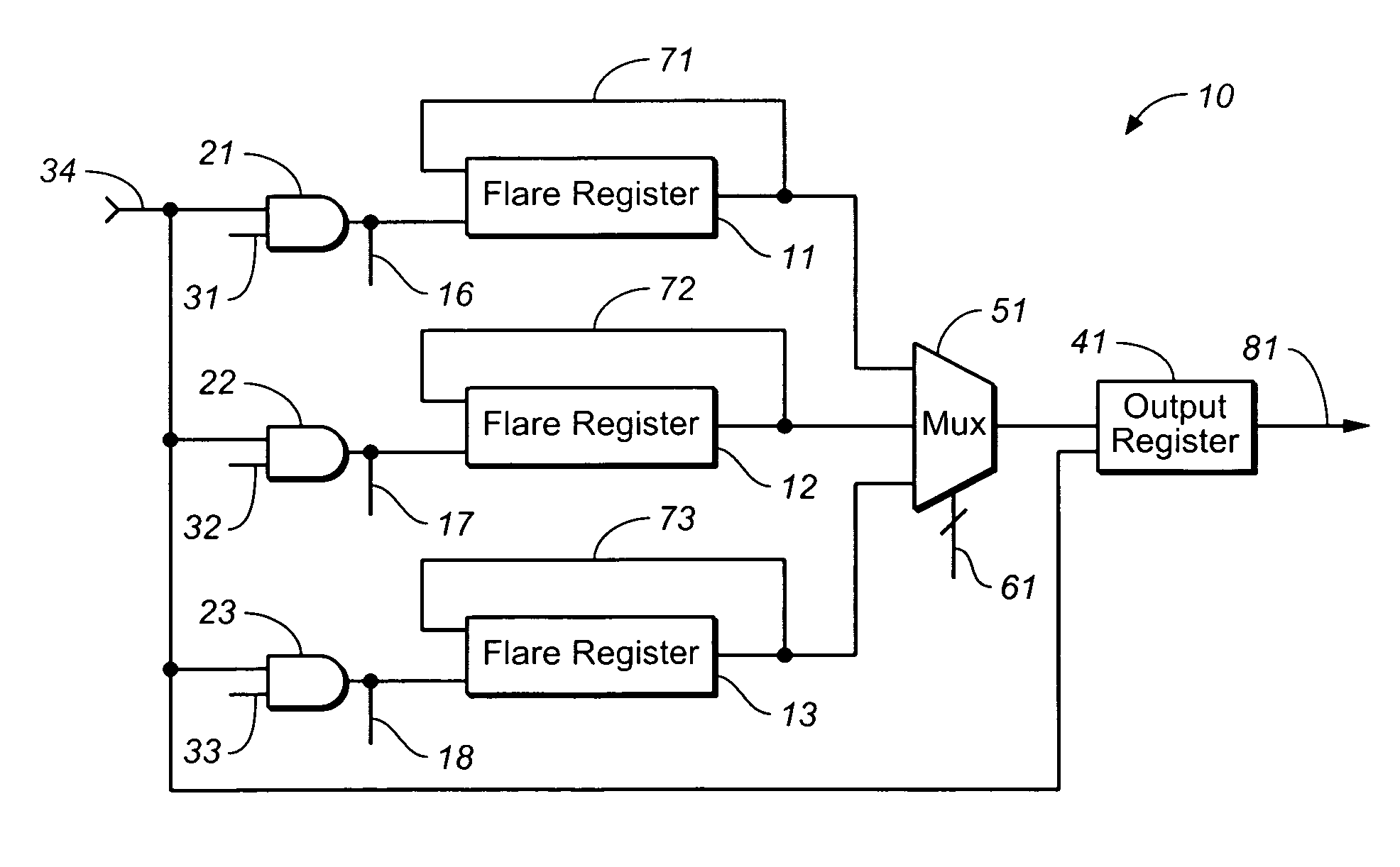
[0016]Referring now to FIG. 2, a schematic diagram of the semiconductor memory testing circuitry 10 constructed according to principles of the present invention is shown. In FIG. 2, flare registers 11, 12 and 13 (which ar...


PUM


Abstract

A semiconductor memory testing implementation suitable for build-in self repair (BISR) memories provides, in one embodiment, a memory testing circuit configuration including an output register for receiving digital data. A plurality of shift registers serially output the digital data to be received by the output register. Each one of the plurality of shift registers includes a feedback path for enabling the digital data output by a corresponding one of the plurality of shift registers to be input back into the corresponding shift register in a same sequence as the digital data is output from the corresponding shift register.

Description

BACKGROUND OF THE INVENTION[0001]1. Field of the Invention[0002]The present invention relates generally to the testing of semiconductor memories, and more particularly to a testing implementation suitable for built-in self-repair (BISR) memories.[0003]2. Description of the Related Art[0004]Integrated circuits have become key components of many consumer and commercial electronic products, often replacing discrete components and enhancing functionality. The semiconductor processing technologies that produce these integrated circuits have advanced to the point where complete systems, including memories, can be reduced to a single integrated circuit or application specific integrated circuit (ASIC) device. It is a common practice for the manufacturers of such integrated circuits to thoroughly test device functionality at the manufacturing site. Because of the increasing complexity of new designs, test development costs can account for a large percentage of the total ASIC development cos...

Claims


Application Information

Patent Timeline
Patent Type & Authority Patents(United States)
IPC IPC(8): G11C29/00G11C7/00B05B1/30F16K31/385
CPCB05B1/3013F16K31/3855B05B1/3026
Inventor PURI, MUKESH K.AGRAWAL, GHASI R.CROSBY, THOMPSON W.
Owner AVAGO TECH INT SALES PTE LTD
Learn More