Electron emitter comprising emitter section made of dielectric material

a dielectric material and emitter technology, applied in the field of electro-emitters, can solve the problems of merely tens of thousands of electrons emitted, complex panel fabrication process, high panel fabrication cost, etc., and achieve the effects of long service life, high reliability, and not easily damaged

Inactive Publication Date: 2007-03-06
NGK INSULATORS LTD
View PDF77 Cites 11 Cited by
  • Summary
  • Abstract
  • Description
  • Claims
  • Application Information

AI Technical Summary

Benefits of technology

[0010]It is an object of the present invention to provide an electron emitter having an emitter section made of a dielectric material in which a

Problems solved by technology

All of these disclosed electron emitters are disadvantageous in that since no dielectric body is employed in the emitter section, a forming process or a micromachining process is required between facing electrodes, a high voltage needs to be applied between the electrodes to emit electrons, and a panel fabrication process is complex and enta

Method used


Image

  • Electron emitter comprising emitter section made of dielectric material
  • Electron emitter comprising emitter section made of dielectric material
  • Electron emitter comprising emitter section made of dielectric material

Examples


first embodiment

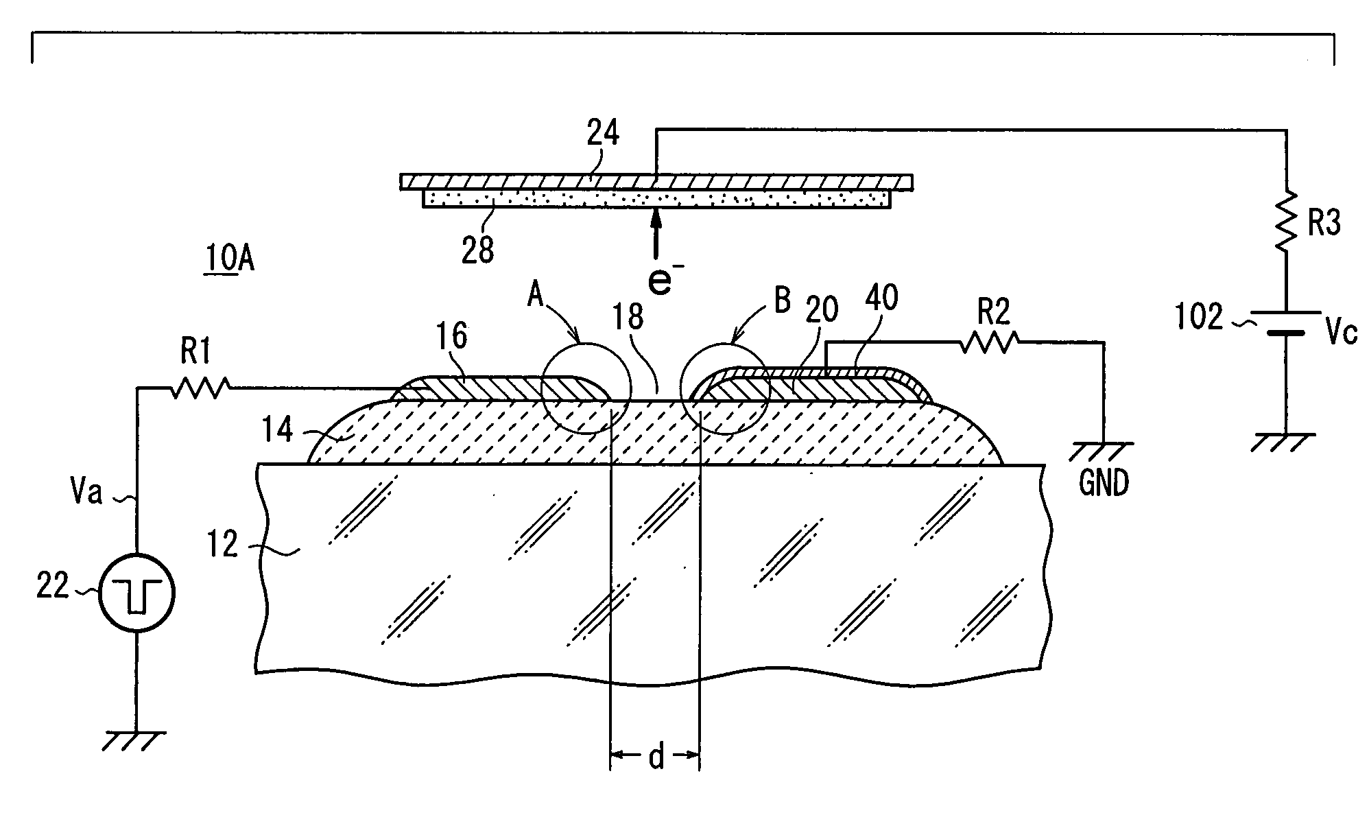
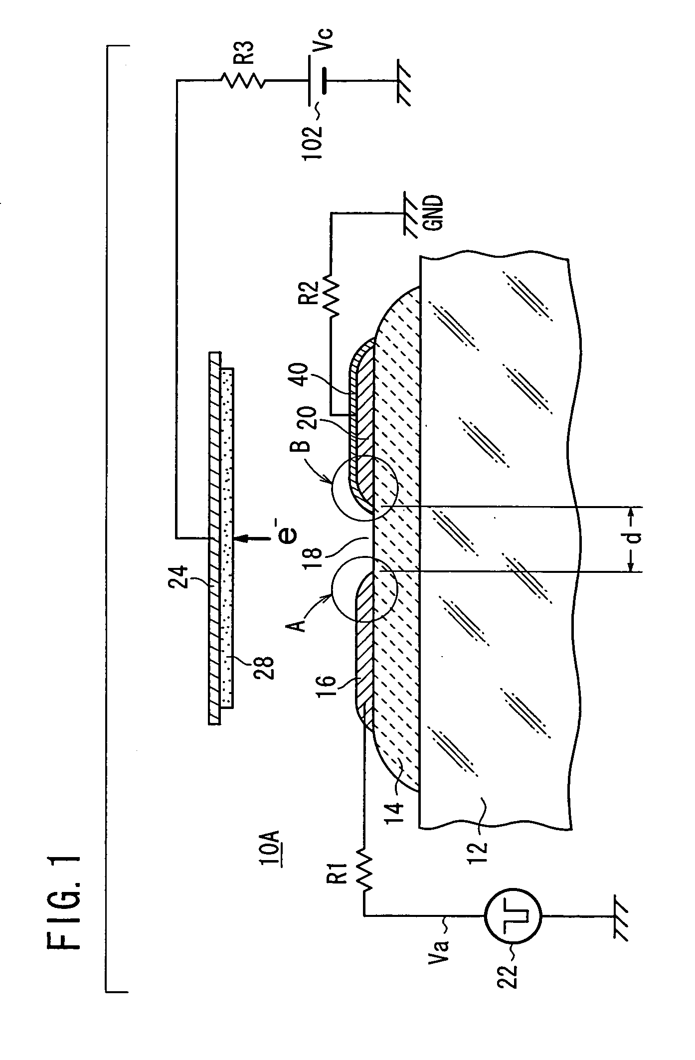
[0059]As shown in FIG. 1, an electron emitter 10A comprises an emitter section 14 formed on a substrate 12, a first electrode (cathode electrode) 16 and a second electrode (anode electrode) 20 formed on one surface of the emitter section 14. A slit 18 is formed between the cathode electrode 16 and the anode electrode 20. A pulse generation source 22 applies a drive voltage Va between the cathode electrode 16 and the anode electrode 20 through a resistor R1. In FIG. 1, the anode electrode 20 is connected to GND (ground) and hence set to a zero potential. However, the anode electrode 20 may be set to a potential other than the zero potential.

[0060]For using the electron emitter 10A as a pixel of a display, a third electrode (collector electrode) 24 is provided above the emitter section 14 at a position facing the slit 18, and the collector electrode 24 is coated with a fluorescent layer 28. A bias voltage source 102 (having a bias voltage Vc) is connected to the collector electrode 2...

second embodiment

[0122]Next, an electron emitter 10B will be described with reference to FIG. 11.

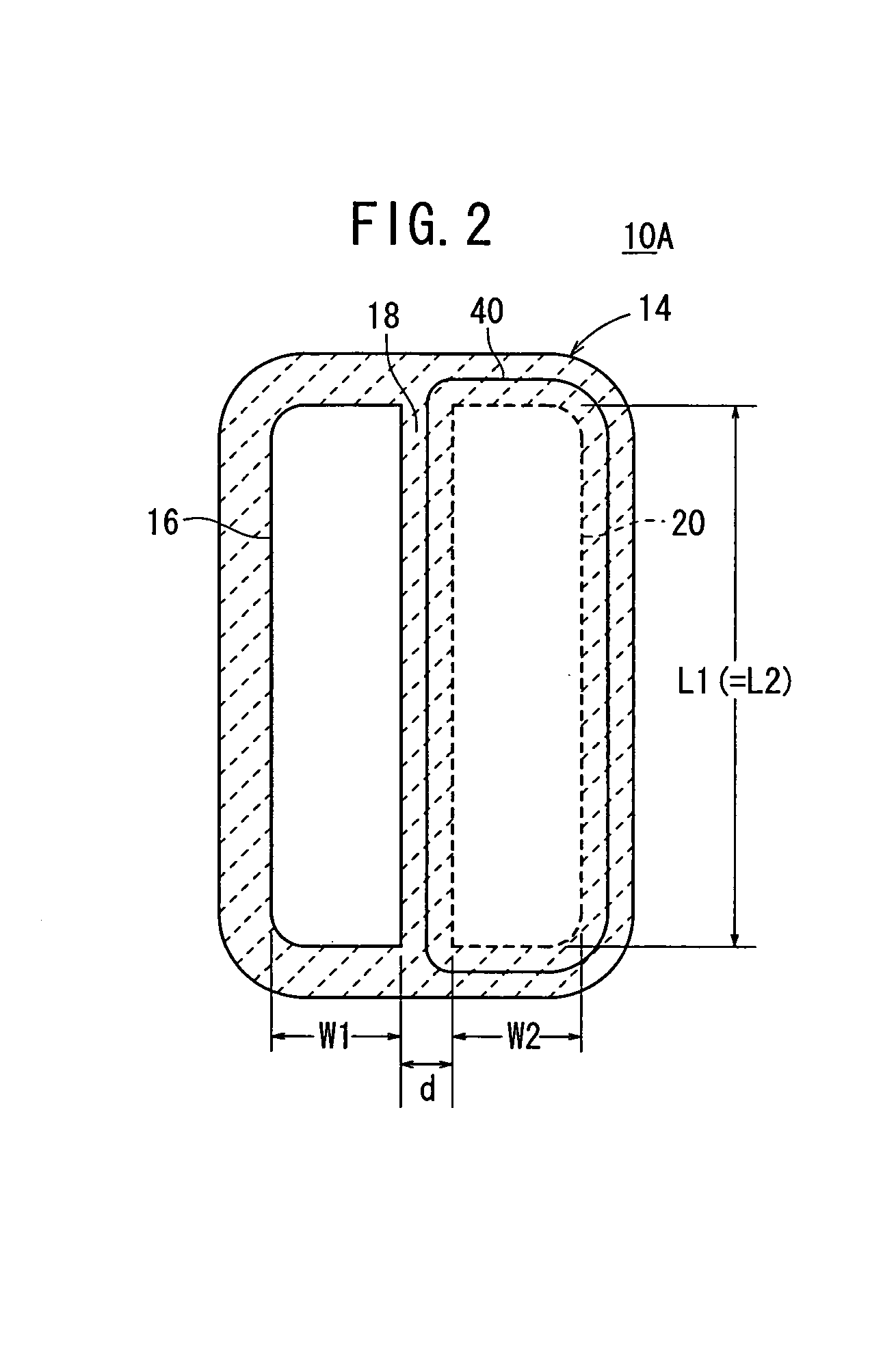
[0123]As shown in FIG. 11, the electron emitter 10B according to the second embodiment includes an emitter section 14 having a width d in the range of 0.1 to 50 μm. A cathode electrode 16 is formed on one side of the emitter section 14, and an anode electrode 20 is formed on the other side of the emitter section 14. The emitter section 14 is formed in a slit 18 between the cathode electrode 16 and the anode electrode 20, and the emitter section 14 is sandwiched between the cathode electrode 16 and the anode electrode 20.

[0124]As with the first embodiment, a charging film 40 is formed on the surface of the anode electrode 20. As shown in FIG. 11, a protective film 42 may be formed on the cathode electrode 16.

[0125]In the electron emitter 10B according to the second embodiment, as with the electron emitter 10A according to the first embodiment, damage to the cathode electrode 16 is prevented. Since the em...


PUM


Abstract

An electron emitter has an emitter section formed on a substrate, and a cathode electrode and an anode electrode formed on a same surface of the emitter section. A slit is formed between the cathode electrode and the anode electrode. A drive voltage from a pulse generation source is applied between the anode electrode and the cathode electrode. The anode electrode is connected to the ground. A charging film is formed on a surface of the anode electrode.

Description

CROSS REFERENCE TO RELATED APPLICATION[0001]This application is a continuation-in-part application of U.S. application Ser. No. 10 / 405,955 filed May 02, 2003, which is now abandoned, and claims the benefit of Japanese Application 2002-348900, filed Nov. 29, 2002, and Japanese Application 2003-154528, filed May 30, 2003, the entireties of which are incorporated herein by reference.BACKGROUND OF THE INVENTION[0002]1. Field of the Invention[0003]The present invention relates to an electron emitter including a first electrode and a second electrode formed on an emitter section. A slit is formed between the first electrode and the second electrode.[0004]2. Description of the Related Art[0005]In recent years, electron emitters having a cathode electrode and an anode electrode have been used in various applications such as field emission displays (FEDs) and backlight units. In an FED, a plurality of electron emitters are arranged in a two-dimensional array, and a plurality of fluorescent e...

Claims


Application Information

Patent Timeline
IPC IPC(8): H01J1/62H01J1/30H01J1/32
CPCH01J1/32H01J1/30
Inventor TAKEUCHI, YUKIHISANANATAKI, TSUTOMUOHWADA, IWAO
Owner NGK INSULATORS LTD
Why Eureka
Try Eureka