Semiconductor integrated circuit having discrete trap type memory cells

a technology of integrated circuits and memory cells, which is applied in the direction of semiconductor devices, solid-state devices, instruments, etc., can solve the problems of deterioration of signal margins, and achieve the effects of reducing the channel current needed for program execution, reducing the storage charge for detection, and increasing programming efficiency

Inactive Publication Date: 2007-03-13
RENESAS ELECTRONICS CORP
View PDF17 Cites 4 Cited by
  • Summary
  • Abstract
  • Description
  • Claims
  • Application Information

AI Technical Summary

Benefits of technology

[0026]Accordingly, it is an object of the present invention to provide a semiconductor integrated circuit having a nonvolatile memory which has less possibility of detecting a surface current other than a channel current detected through a predetermined channel.
[0034]A switch transistor, which is necessary to realize the source side injection, is formed in a memory cell together with a memory transistor by self-aligned diffusion, thereby suppressing an increase in area. Further, the line of the switch transistor is devised to shut off the flow of a surface current, which is flown due to a virtual ground, to a source line / bit line.

Problems solved by technology

Further, disturb is applied to an unselected cell as read is accumulated, whereby a signal margin is liable to be deteriorated.

Method used


Image

  • Semiconductor integrated circuit having discrete trap type memory cells
  • Semiconductor integrated circuit having discrete trap type memory cells
  • Semiconductor integrated circuit having discrete trap type memory cells

Examples


seventh embodiment

of Memory Cell>

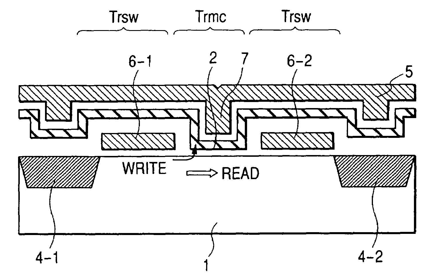
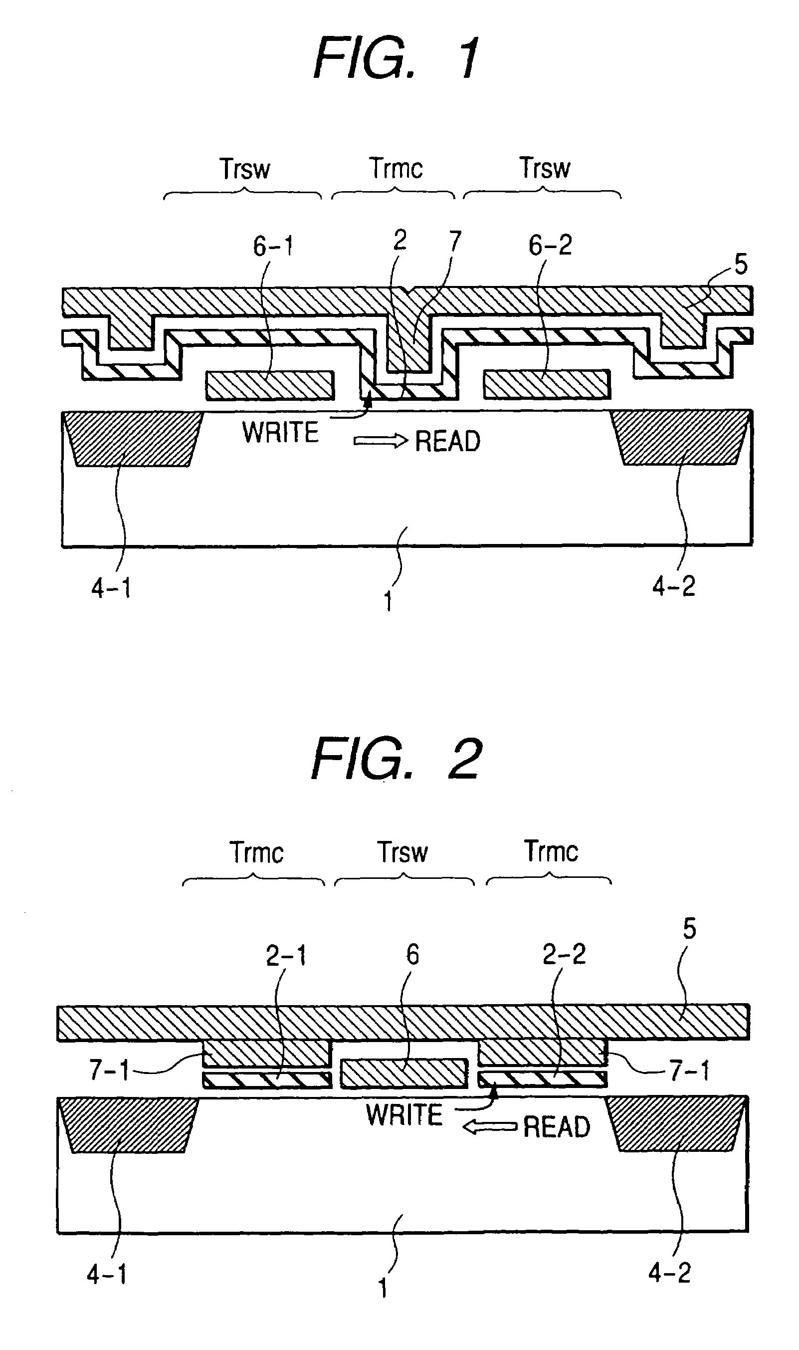
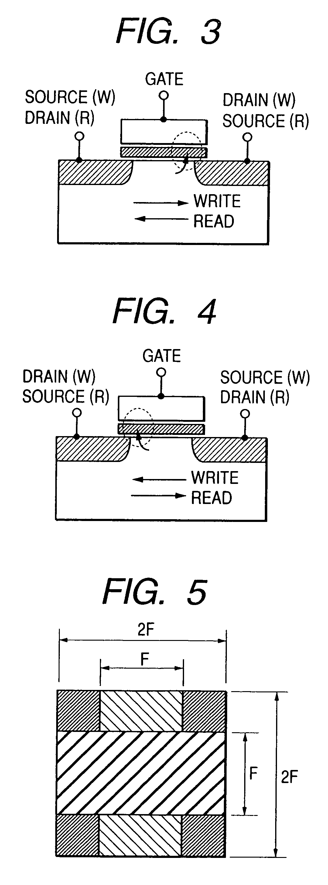
[0235]FIG. 109 shows a cross section of a memory cell according to a seventh embodiment. The memory cell shown in the figure is arranged such that the memory gate electrodes 2-1 and 2-2 of memory transistors Trmc are connected to a word line 5, and the memory transistors Trmc are formed on both the side walls of the switch gate electrode 6A of a switch transistor Trsw using a side wall technology. With this arrangement, the memory cell having an area of about 3F2 can be realized.

[0236]FIGS. 110 to 114 schematically show the cross sections of a device at stages in a manufacturing process of memory cells according to the seventh embodiment described with reference to FIG. 109.

[0237]FIG. 110 shows a structure in which the gate insulating film 71 for the switch transistor Trsw, an electrode material 75 of the switch gate electrode 6A, an interlayer insulating film 73, and an interlayer protection film 74 are deposited. A silicon thermal oxide thin film having a thickness ...


PUM


Abstract

A multi-storage nonvolatile memory of high density, high speed and high reliability has a memory transistor and switch transistors disposed on both the sides of the memory transistor. The memory transistor includes a gate insulating film having discrete traps and a memory gate electrode, whereas the switch transistors include switch gate electrodes. The gate insulating film has the discrete traps for storing information charge, can locally inject carriers, and one memory cell constitutes a multi-storage cell for storing at least information of 2 bits. The switch transistors having the switch gate electrodes realize source side injection. The memory transistor is fommed together with the switch transistors in self-aligned diffusion. The memory gate electrode of the memory transistor is connected to a word line so as to perform word-line erase.

Description

[0001]This is a continuation application of U.S. Ser. No. 11 / 126,236, filed May 11, 2005 now U.S. Pat. No. 7,012,296 which is a continuation application of U.S. Ser. No. 10 / 663,779, filed Sep. 17, 2003 (now U.S. Pat. No. 6,894,344); which is a continuation of application U.S. Ser. No. 10 / 377,785, filed Mar. 4, 2003 (now U.S. Pat. No. 6,674,122), which is a continuation of U.S. Ser. No. 09 / 660,923, filed Sep. 13, 2000 (now U.S. Pat. No. 6,531,735).BACKGROUND OF THE INVENTION[0002]The present invention relates to a nonvolatile semiconductor memory device having multi-storage nonvolatile memory cells in which one memory cell transistor can store information of at least two bits, and further to a semiconductor integrated circuit such as a microcomputer and the like containing the nonvolatile semiconductor memory device.[0003]A typical nonvolatile semiconductor memory device having nonvolatile memory cells is an EEPROM (electrically erasable and programmable read only memory), which can ...

Claims


Application Information

Patent Timeline
Patent Type & Authority Patents(United States)
IPC IPC(8): H01L29/788
CPCG11C16/0475H01L27/115H01L29/7887H01L27/11524H01L29/42332H01L27/11521H10B41/35H10B69/00H10B41/30
Inventor KAMIGAKI, YOSHIAKIMINAMI, SHINICHIKATAYAMA, KOZOKATO, MASATAKA
Owner RENESAS ELECTRONICS CORP
Why Eureka
Try Eureka