Semiconductor device producing apparatus and producing method of semiconductor device

a technology of semiconductor devices and producing apparatus, which is applied in the direction of packaging, transportation and packaging, packaging goods types, etc., can solve the problems of natural oxide film, adverse effect of control on film thickness variation of the processing of the wafer, and unintended oxide film (natural oxide film, etc.) in terms of control, and achieve the effect of shortening the standby tim

Inactive Publication Date: 2007-04-03
KOKUSA ELECTRIC CO LTD
View PDF27 Cites 305 Cited by
  • Summary
  • Abstract
  • Description
  • Claims
  • Application Information

AI Technical Summary

Benefits of technology

[0007]It is, therefore, a main object of the present invention to provide a semiconductor device producing apparatus and a producing method of a semiconductor device which are capable of shortening a standby time required until a substrate or substrates are transferred into a processing chamber to prevent natural oxide film or films from being generated on the substrate or the substrates

Problems solved by technology

If the group of new wafers transferred to the second boat is exposed to atmosphere outside the processing chamber, an unintended oxide film (natural oxide film, hereinafter) in terms of control is adversely formed on a surface of the wafer by moisture and oxygen existing in atmosphere.
This natural oxide film exerts an adverse effect on variation of film-thickness processed by a wafer, or increases a contact resistance.

Method used


Image

  • Semiconductor device producing apparatus and producing method of semiconductor device
  • Semiconductor device producing apparatus and producing method of semiconductor device
  • Semiconductor device producing apparatus and producing method of semiconductor device

Examples


first embodiment

(First Embodiment)

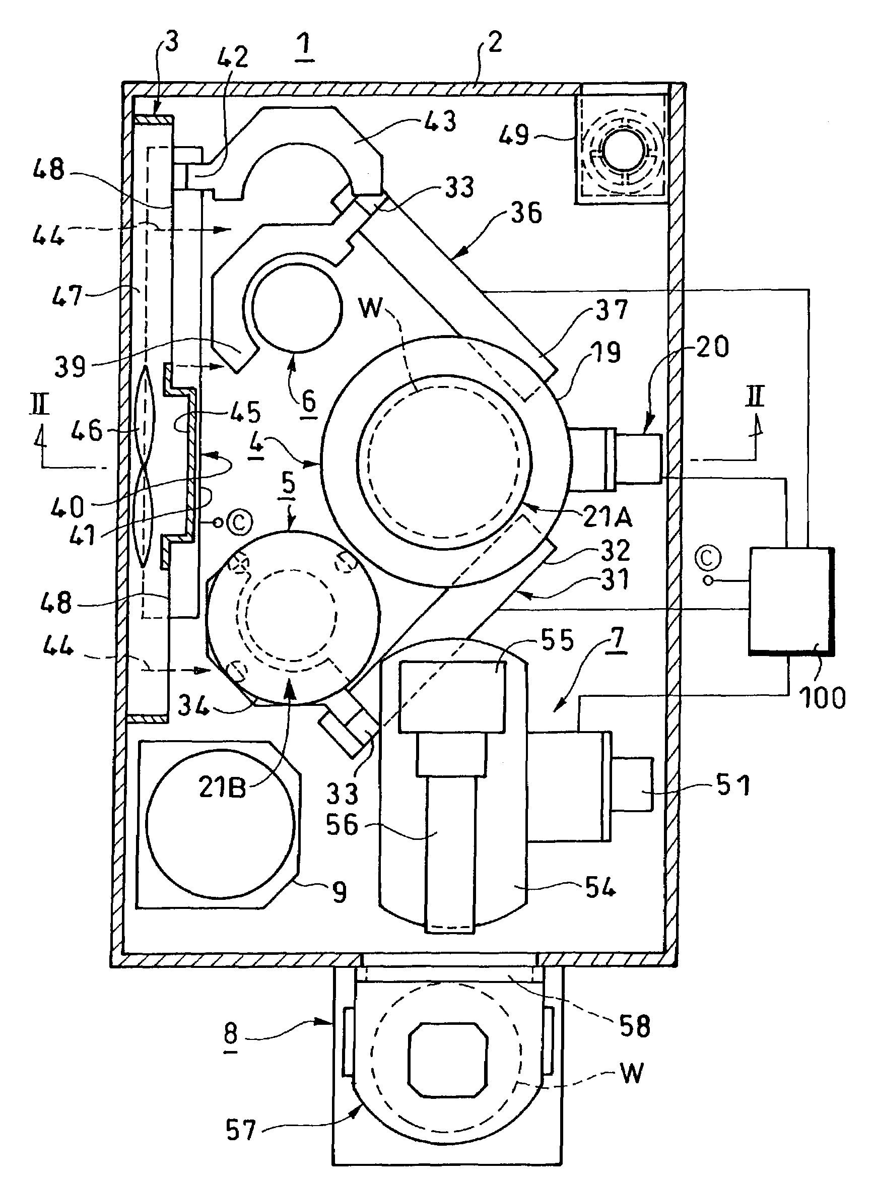
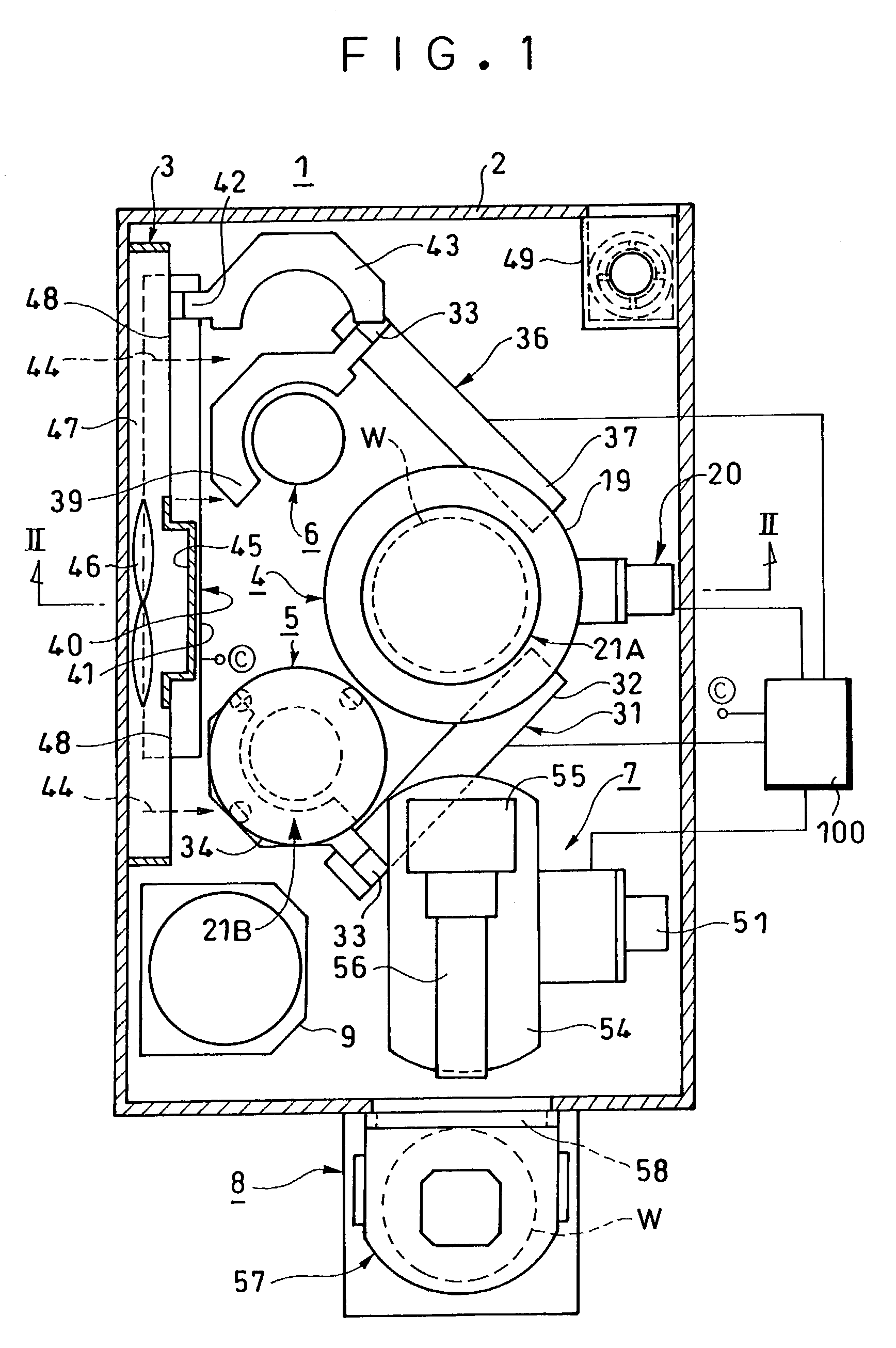
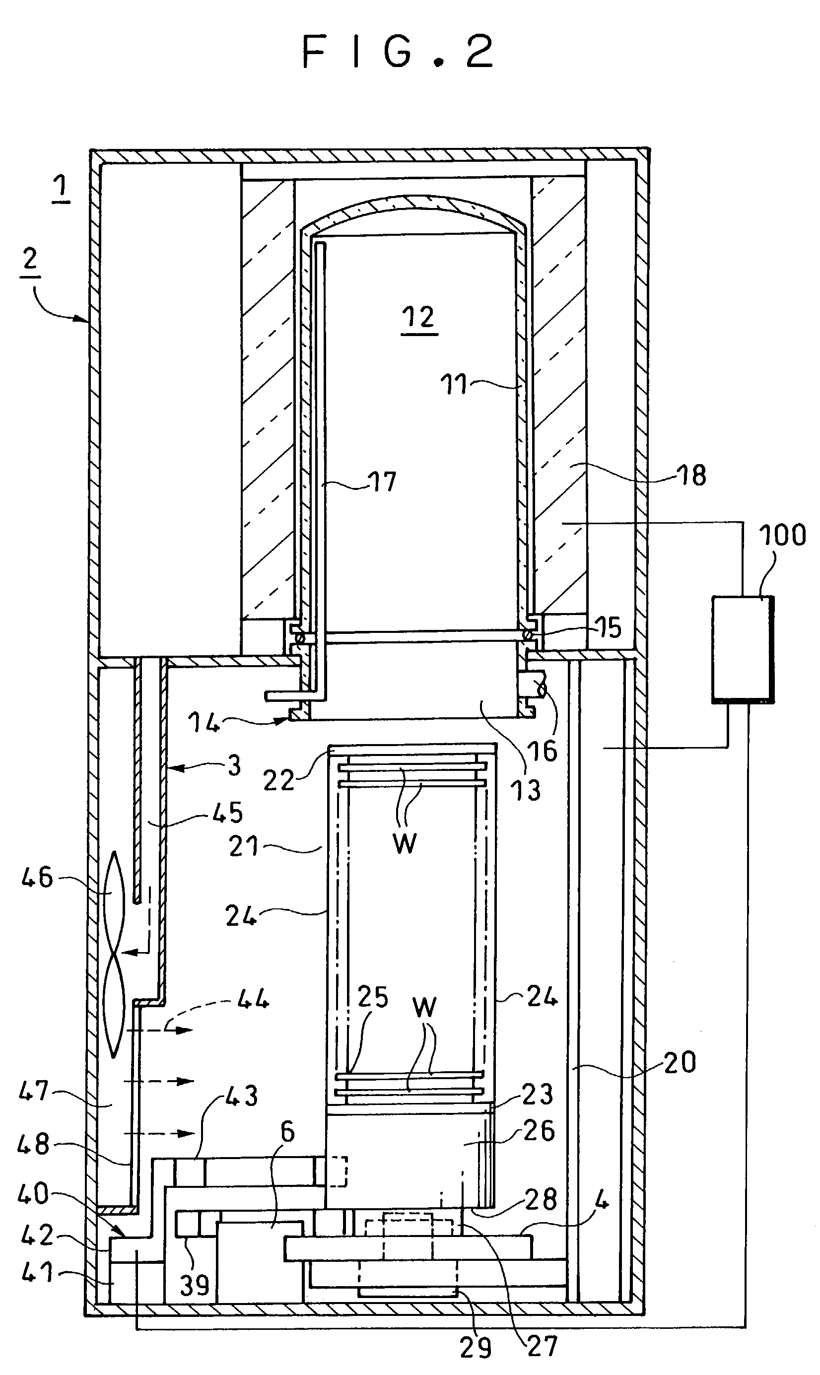
[0034]In this embodiment, a semiconductor device producing apparatus according to the present invention is constituted as a batch-type vertical hot wall CVD (Chemical Vapor Deposition) apparatus (CVD apparatus, hereinafter) as shown in FIG. 1, and is used for subjecting a wafer as a substrate to CVD processing such as annealing processing, oxide film-forming processing, dispersing processing and film-forming processing. In the following explanation, front, rear, left and right are based on FIG. 1. That is, a pod stage 8 side is a front side, a side (cooling stage 6 side) opposed to the pod stage 8 side is a rear side, a clean unit 3 side is a left side, and a side (boat elevator 20 side) opposed to the clean unit 3 side is a right side.

[0035]As shown in FIG. 1, a CVD apparatus 1 according to this embodiment has a case 2 which is formed into a rectangular parallelepiped box having a rectangular shape as viewed from above. A clean unit 3 is disposed on a left sidewal...

second embodiment

(Second Embodiment)

[0060]Next, a second embodiment of the present invention will be explained. The same constituent elements and constituent elements having the same function as in the first embodiment are designated with the same symbols as in the first embodiment.

[0061]A CVD apparatus of the second embodiment is different from that of the first embodiment in that a boat transfer apparatus 60 is provided for transferring the first boat 21A and the second boat 21B between the thermal processing stage 4 and the cooling stage 6 and between the cooling stage 6 and the standby stage 5, instead of the second boat transfer apparatus 36 and the third boat transfer apparatus 40 as shown in FIG. 8. As shown in FIG. 8, the boat transfer apparatus 60 comprises a linear actuator 61 directed in the vertical direction, a rotary actuator 62 which is moved up and down by the linear actuator 61, and an arm 63 which reciprocates in a horizontal plane by the rotary actuator 62 such as to draw an arc o...


PUM

PropertyMeasurementUnit
timeaaaaaaaaaa
temperatureaaaaaaaaaa

Abstract

A semiconductor device producing apparatus is disclosed. The apparatus includes a carrier-holding stage for placing a carrier; first, second and third stages each for holding first and second boats one at a time, each boat holding one or more substrates; a boat transfer mechanism for transferring the boats among the first, second and third stages; and a substrate transfer mechanism for transferring the substrate(s) from the carrier to the boat held by the first stage. A controller controls the first stage, the boat transfer mechanism and the substrate transfer mechanism so that the boat transfer mechanism transfers one of the boats from the second stage to the first stage, the substrate transfer mechanism then transfers the substrate(s) from the carrier to the boat held by the first stage, and the first stage then moves the boat into the processing chamber for processing.

Description

BACKGROUND OF THE INVENTION[0001]1. Field of the Invention[0002]The present invention relates to a semiconductor device producing apparatus and a producing method of a semiconductor device, and more particularly, to a semiconductor device producing apparatus and a producing method of a semiconductor device which are effectively utilized for subjecting a semiconductor wafer or semiconductor wafers to thermal processing such as annealing processing, oxide film-forming processing, diffusion processing and film-forming processing.[0003]2. Description of the Related Art[0004]Generally, in a producing method of a semiconductor device, a batch-type vertical hot wall thermal processing apparatus (thermal processing apparatus, hereinafter) is widely used for subjecting a semiconductor wafer (wafer, hereinafter) into which an integrated circuit including a semiconductor element is incorporated to thermal processing such as annealing processing, oxide film-forming processing, diffusion process...

Claims


Application Information

Patent Timeline
Patent Type & Authority Patents(United States)
IPC IPC(8): H01L21/677B65B21/02B65B69/00B65G65/34C23C16/44
CPCH01L21/67757Y10S414/137Y10S414/139
Inventor MORIMITSU, KAZUHIROMATSUNAGA, TATSUHISAKANEKO, MASANORINOTO, KOUICHIYANAGAWA, HIDEHIROMATSUSHIMA, MASAKI
Owner KOKUSA ELECTRIC CO LTD
Why Eureka
Try Eureka