

Semiconductor device and manufacturing method thereof including a probe test step and a burn-in test step
a technology of semiconductor devices and manufacturing methods, applied in the direction of individual semiconductor device testing, semiconductor/solid-state device testing/measurement, instruments, etc., can solve the problems of increasing sliding frictional force of pivots, increasing pressure, and unable to follow relative gradients, so as to suppress the dispersion of load and enhance the reliability and productivity of integrated circuits.
- Summary
- Abstract
- Description
- Claims
- Application Information
AI Technical Summary
Benefits of technology
Problems solved by technology
Method used
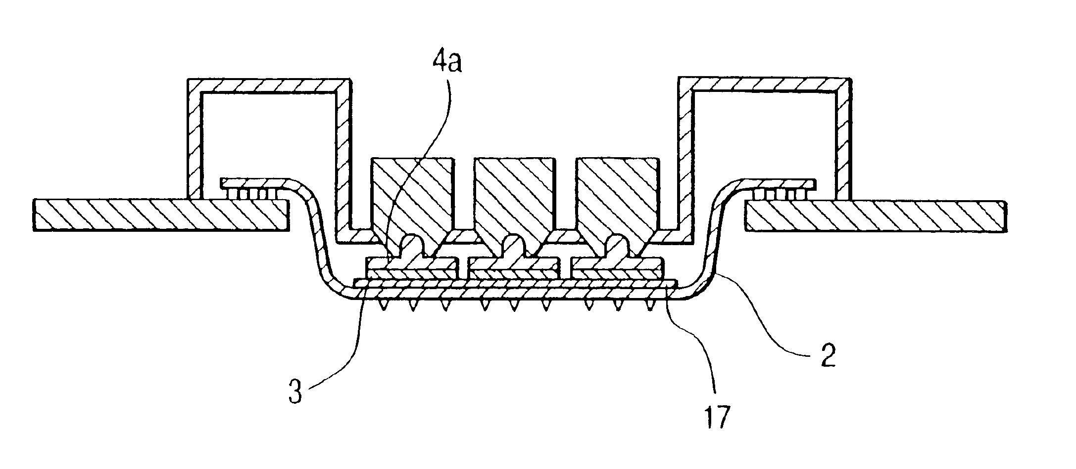
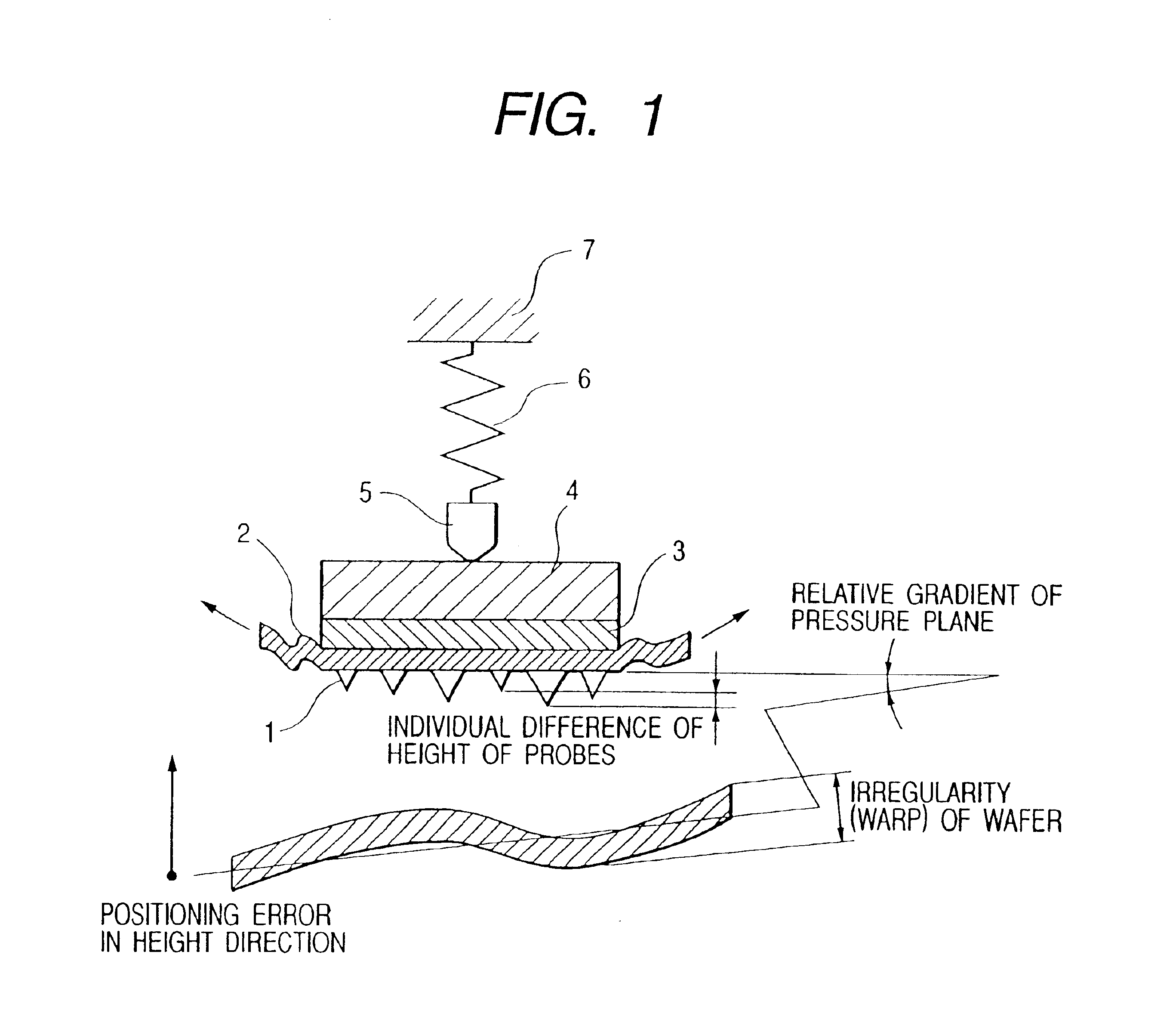
Image

Examples
Embodiment Construction
[0084]Preferred embodiments of the present invention will be explained below with reference to the drawings.
[0085]Semiconductor devices are manufactured through the following steps in the present embodiment:[0086]Integrated circuit forming step for forming a large number of integrated circuits on a wafer;[0087]Probe test step for probing (test on conductivity) the wafer on which the large number of integrated circuits have been formed;[0088]Burn-in test step for implementing a burning-in test (thermal load test) on the wafer on which the large number of integrated circuits have been formed; and[0089]Dicing step for dicing the wafer into a plurality of chips (cutting individual integrated circuits) after completion of the probe test step and the burn-in test step. Each of the steps will be explained below in detail.
[Integrated circuit Forming Step]
[0090]Integrated circuits are formed while undergoing many unit steps per specification of the integrated circuits to be manufactured on a...
PUM
 Abstract
Description
Claims
Application Information