Method utilizing compensation features in semiconductor processing

a semiconductor and compensation feature technology, applied in the field of photolithography and etching processes in semiconductor devices, can solve the problems of insufficient elimination of proximity effects, corresponding and undesirable pattern formation in photoresist layers, etc., and achieve the effect of widening the process window and reducing the depth of focus and proximity effects

Inactive Publication Date: 2007-04-10
TAIWAN SEMICON MFG CO LTD
View PDF11 Cites 240 Cited by
  • Summary
  • Abstract
  • Description
  • Claims
  • Application Information

AI Technical Summary

Benefits of technology

[0008]To address these and other objects, and in view of its purposes, the present invention provides a method for mitigating depth of focus and proximity effects during photolithography and etch processes, thereby widening the process window for such photolithography processes.

Problems solved by technology

When the light beam passes through the photoresist layer on the substrate, it also reflects off the substructure beneath the photoresist layer and the phenomenon of interference results.
These exposure phenomenon combine to create the proximity effect which causes problems when isolated lines and nested, i.e., densely packed, lines undergo exposure at the same time.
If the scattering bars are not wide enough, they do not sufficiently eliminate the proximity effect or compensate for depth of focus concerns that arise between features at different topographical levels of the device being exposed.
Conversely, if the scattering bars are too wide, they undesirably cause a corresponding and undesirable pattern to be formed in the photoresist layer.

Method used


Image

  • Method utilizing compensation features in semiconductor processing
  • Method utilizing compensation features in semiconductor processing
  • Method utilizing compensation features in semiconductor processing

Examples


Embodiment Construction

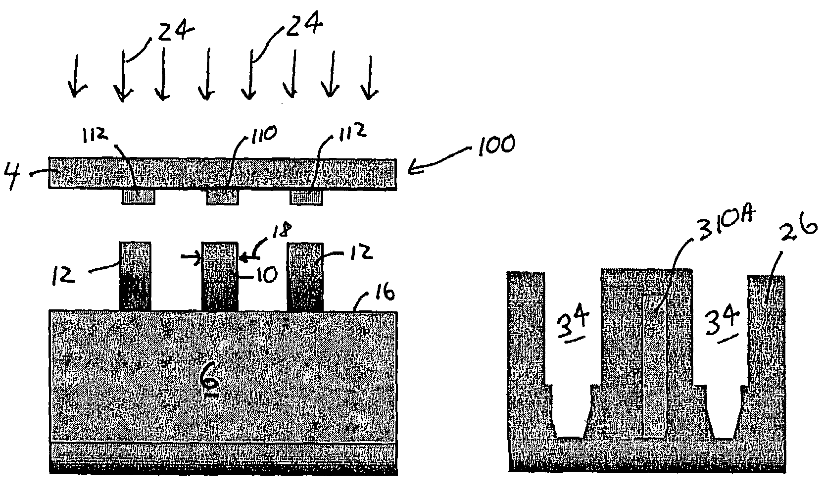
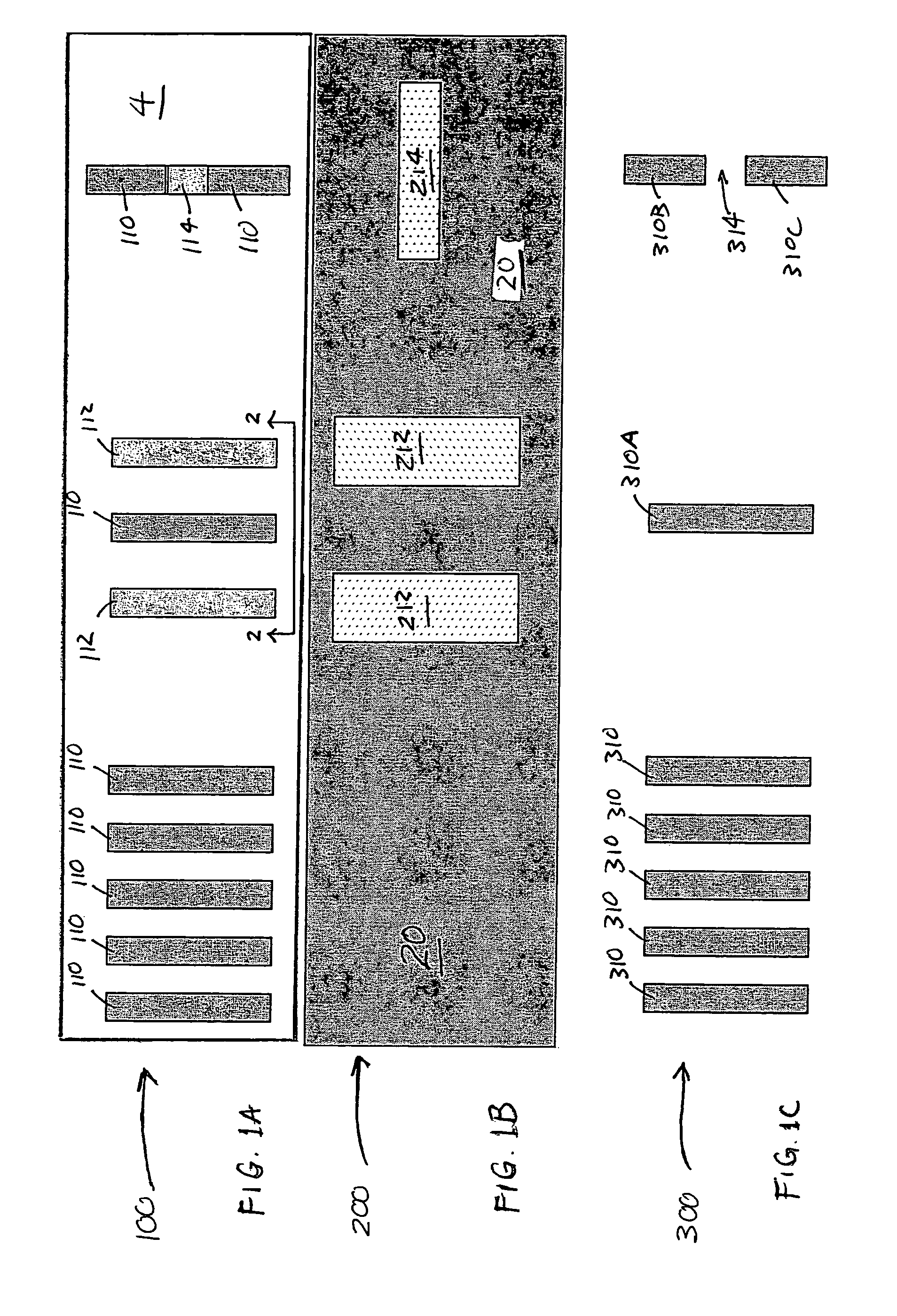
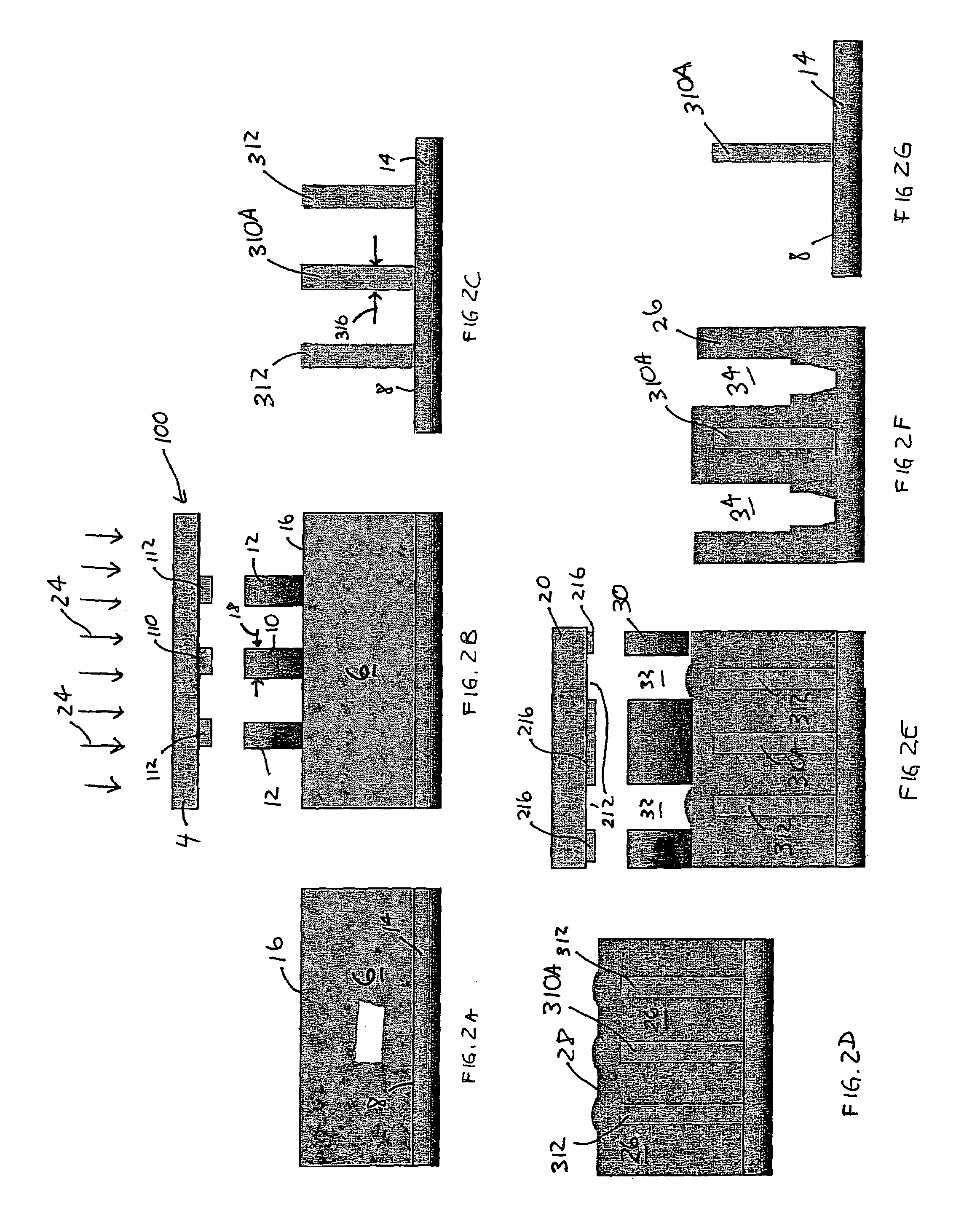
[0015]The present invention overcomes the limitations of the prior art and provides compensation features such as scattering bars added to a photomask pattern. The compensation features are patterned and etched along with device features, then removed. The compensation features may be used at any of various mask levels and in conjunction with the production of various semiconductor devices. In one embodiment, the compensation features may be scattering bars used in conjunction with an isolated line or an outermost line of an array of lines. The compensation feature is sufficiently wide to improve the depth of focus for isolated or outermost lines of the desired pattern which are situated differently than otherwise similar nested lines. In an another embodiment, the compensation feature may be a line segment connecting two linearly aligned device features. When this exemplary compensation feature is removed, the facing end lines include superior pattern integrity. The method of the p...


PUM

PropertyMeasurementUnit
widthaaaaaaaaaa
areaaaaaaaaaaa
etch rateaaaaaaaaaa

Abstract

A photolithography and etch process sequence includes a photomask having a pattern with compensation features that alleviate patterning variations due to the proximity effect and depth of focus concerns during photolithography. The compensation features may be disposed near isolated or outermost lines of a device pattern. A photoresist pattern is formed to include the compensation features and the pattern etched to form a corresponding etched pattern including the compensation features. After etching, a protection material is formed over the layer and a trim mask is used to form a further photoresist pattern over the protection material. A subsequent etching pattern etches the protection material and removes the compensation features and results in the device lines being formed unaffected by proximity effects. Flare dummies may additionally be added to the mask pattern to increase pattern density and assist in endpoint detection. Flare dummies, like the compensation features, are subsequently removed by a photolithography and etching process sequence.

Description

FIELD OF THE INVENTION[0001]The present invention relates, most generally, to photolithography and etch processes in semiconductor device manufacturing. More particularly, the present invention relates to a method of improving CD uniformity and decreasing proximity effects and line end shortening in semiconductor device patterning.BACKGROUND[0002]In today's rapidly advancing semiconductor manufacturing industry, the demand for increasing levels of device integration requires that device features are made increasingly smaller and in closer proximity to one another. The most critical step in defining and ultimately producing device features are the photolithography and etching operations. As such, higher levels of device integration will likely be attained by technological advances in the photolithography and / or etch processes. In order to meet this demand, processes for increasing photomask resolution, such as the process of optical proximity correction (OPC), are put forward constan...

Claims


Application Information

Patent Timeline
Patent Type & Authority Patents(United States)
IPC IPC(8): H01L21/308G03F1/00G03F7/40G03C5/00G03F1/14G03F9/00H01L21/469
CPCG03F1/144G03F1/36Y10S430/151G03F1/70
Inventor CHEN, KUEI SHUNLIN, CHIN-HSIANGCHIU, CHIH-CHENG
Owner TAIWAN SEMICON MFG CO LTD
Why Eureka
Try Eureka