

Diode stack high voltage regulator
a high-voltage regulator and diode stack technology, applied in the direction of electrical variable regulation, process and machine control, instruments, etc., can solve the problems of slow recovery time, instability of the regulator, and another stability/recovery time problem, so as to reduce the feedback delay, and increase the gain of the diode stack
- Summary
- Abstract
- Description
- Claims
- Application Information
AI Technical Summary
Benefits of technology
Problems solved by technology
Method used
Image

Examples
Embodiment Construction
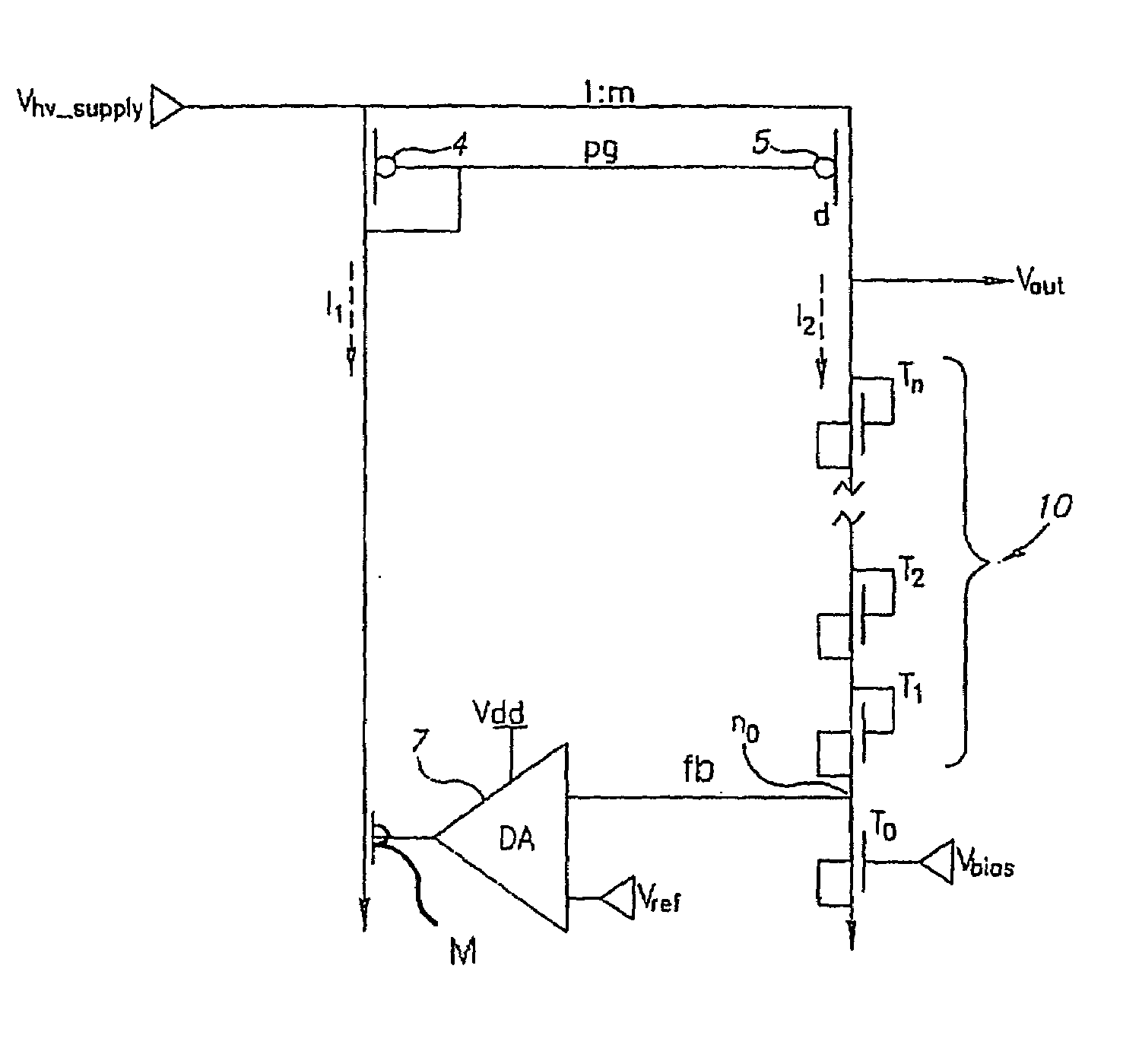
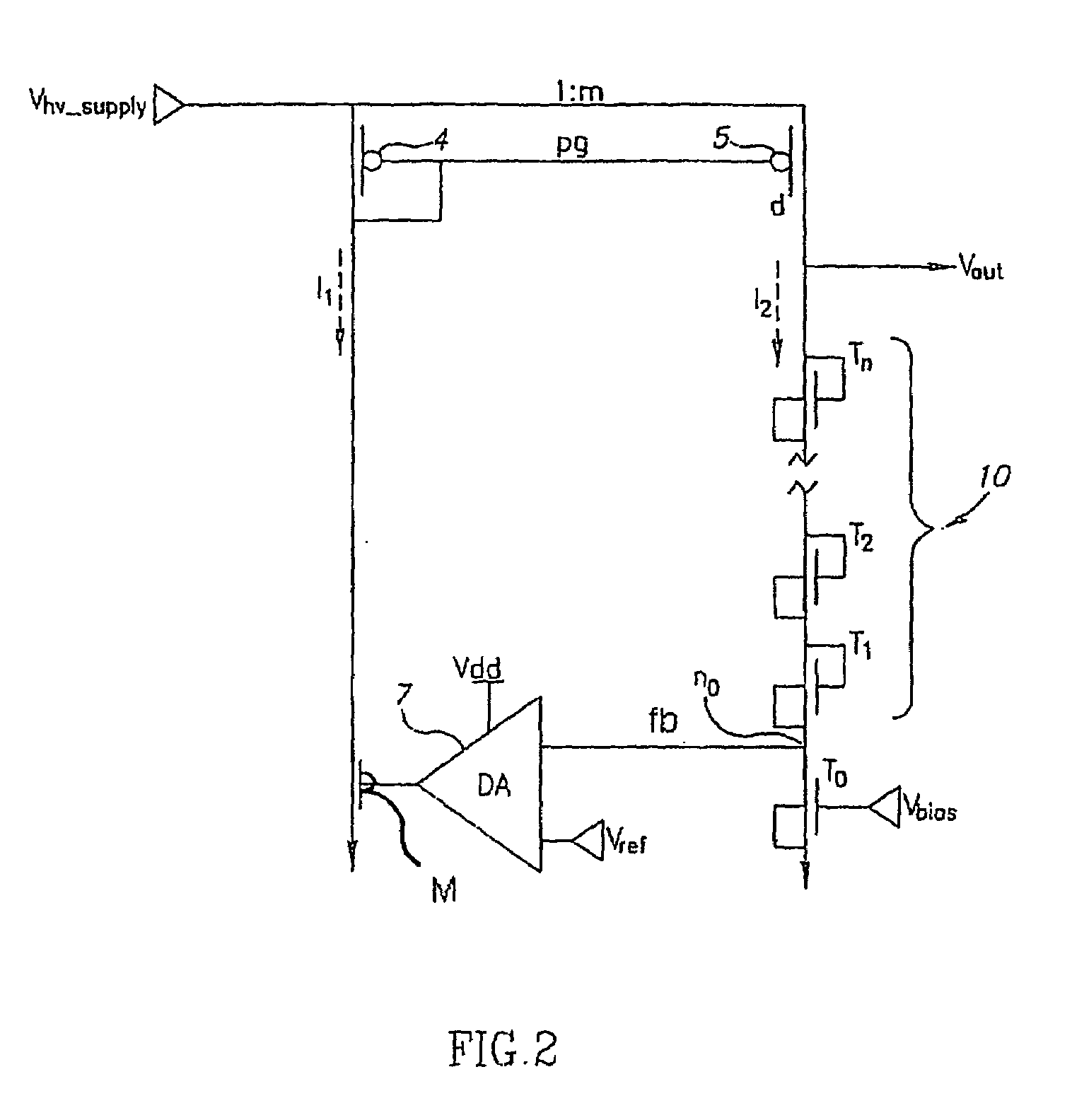
[0020]Reference is now made to FIG. 2, which illustrates a simplified block diagram of a high voltage regulator, in accordance with an embodiment of the present invention. Components of the circuitry of FIG. 2 that are similar to that of FIG. 1 are designated with the same reference labels, and the description is not repeated for the sake of brevity.
[0021]The divider 6 of the architecture of FIG. 1 is replaced in the non-limiting embodiment of FIG. 2 with a diode stack 10. Diode stack 10 may include a plurality of serially connected NMOS transistors T0, T1, T2, . . . Tn. The drain of transistor Tn is connected to the drain of PMOS transistor 5. The gate of transistor Tn is connected to its drain. The source of transistor Tn is connected to its bulk and to the drain of the next NMOS transistor Tn-1. The source of transistor T1 is connected to node n0. The drain of another NMOS transistor T0 is connected to node n0. The gate of transistor T0 receives an input Vbias. The source of tran...
PUM
 Abstract
Description
Claims
Application Information