
Diode stack high voltage regulator

Active Publication Date: 2007-03-29
SAIFUN SEMICON
View PDF3 Cites 5 Cited by
  • Summary
  • Abstract
  • Description
  • Claims
  • Application Information

AI Technical Summary

Benefits of technology

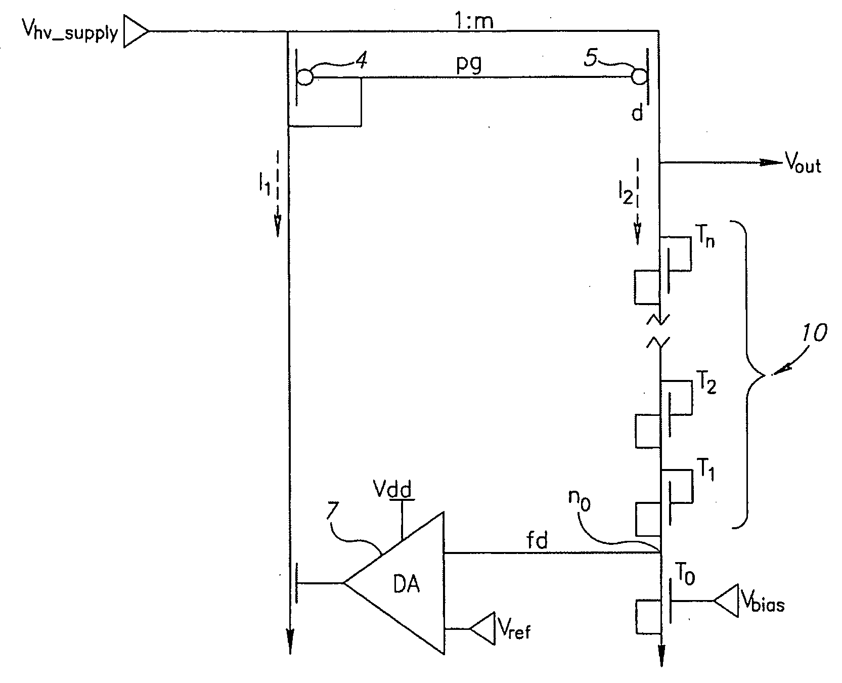
[0010] The present invention seeks to provide a novel high voltage regulator with a diode stack, as is described more in detail hereinbelow. The present invention may have a large diode stack gain (=1) but lower GDA*GNMOS*m, resulting in a generally constant feedback (loop) gain Gloop. The invention has lower feedback delay, better stability and faster recovery time than the prior art.

Problems solved by technology

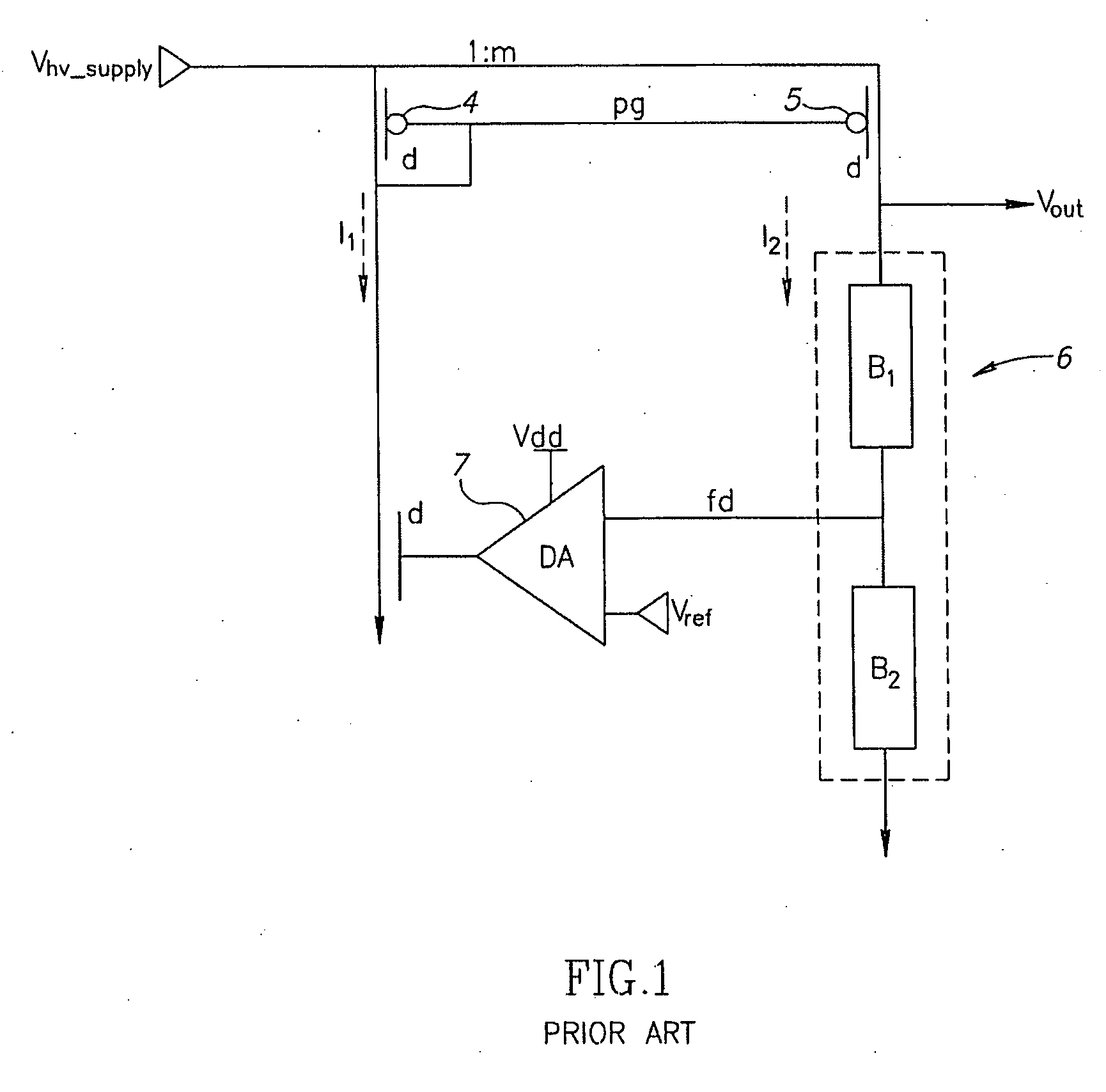
There is an inherent stability problem with the prior art voltage regulator of FIG. 1, because a high loop gain (although having a fast recovery time) leads to instability of the regulator.
On the other hand, a low loop gain results in a slow recovery time.
In the case of a resistor divider, there may be a problem of parasitic capacitance to ground of the resistors, leading to another stability / recovery time problem.
An additional capacitor divider problem is that of parasitic capacitance to ground which adversely affects the accuracy of Vout.
An additional diode divider problem is that it is not possible to have an arbitrary Vout without significantly changing I2.

Method used


Image

  • Diode stack high voltage regulator
  • Diode stack high voltage regulator
  • Diode stack high voltage regulator

Examples


Embodiment Construction

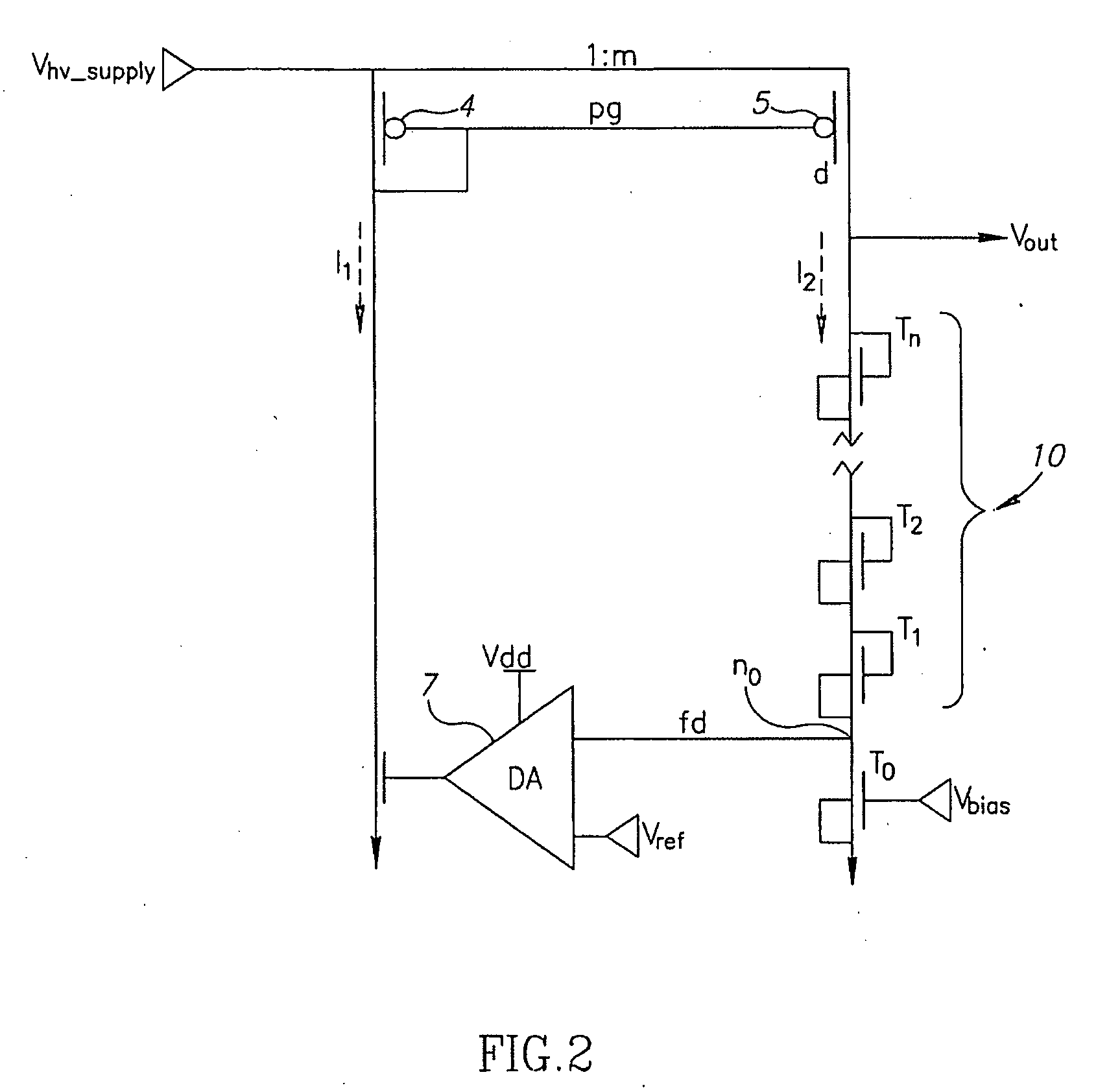
[0019] Reference is now made to FIG. 2, which illustrates a simplified block diagram of a high voltage regulator, in accordance with an embodiment of the present invention. Components of the circuitry of FIG. 2 that are similar to that of FIG. 1 are designated with the same reference labels, and the description is not repeated for the sake of brevity.

[0020] The divider 6 of the architecture of FIG. 1 is replaced in the non-limiting embodiment of FIG. 2 with a diode stack 10. Diode stack 10 may include a plurality of serially connected NMOS transistors T0, T1, T2, . . . Tn. The drain of transistor Tn is connected to the drain of PMOS transistor 5. The gate of transistor Tn is connected to its drain. The source of transistor Tn is connected to its bulk and to the drain of the next NMOS transistor Tn−1. The source of transistor T1 is connected to node n0. The drain of another NMOS transistor T0 is connected to node n0. The gate of transistor T0 receives an input Vbias. The source of t...


PUM


Abstract

A high voltage regulator including a current mirror including a pair of transistors, one of the transistors being connected to a node that outputs an output voltage Vout, a diode stack that includes a plurality of serially connected transistors T0, T1, T2, . . . Tn, wherein the transistor T1 is connected to a node n0, to which is connected another transistor T0 that receives an input bias voltage Vbias, and wherein a feedback voltage fb from node n0 is fed to an input of the differential amplifier, the differential amplifier receiving an input reference voltage Vref at one of its other inputs, and is also connected to positive voltage supply Vdd, the differential amplifier outputting to an NMOS transistor M, and wherein the high voltage regulator has a large diode stack gain and lower GDA*GNMOS*m, resulting in a generally constant feedback (loop) gain Gloop wherein the loop gain is given by: Loop Gain=Gloop=Gstack*GDA*GNMOS*m wherein m is the ratio of the two currents I1 and I2, that is, I2=mI1, Gstack is the gain of the diode stack, GDA is the gain of the differential amplifier and GNMOS is the gain of the NMOS transistor M.

Description

FIELD OF THE INVENTION [0001] The present invention relates generally to voltage regulators, and particularly to a high voltage regulator with a diode stack instead of a divider, e.g., a resistor or capacitor divider. BACKGROUND OF THE INVENTION [0002] Non-volatile memory (NVM) arrays, such as erasable, programmable read only memory (EPROM) or flash memory arrays, or electrically erasable, programmable read only memory (EEPROM) arrays, require high positive or negative voltages to program and erase memory cells of the array. [0003] Read and write operations are typically carried out with voltages that are regulated above a positive voltage supply Vdd. The circuitry that supplies and controls the programming and verification voltages generally comprises a high voltage regulator or high voltage pump (the terms being used herein interchangeably). A typical high voltage regulator architecture is shown in FIG. 1. [0004] A current mirror including a pair of PMOS (p-channel metal oxide sem...

Claims


Application Information

Patent Timeline
IPC IPC(8): G05F3/16
CPCG05F3/262
Inventor DADASHEV, OLEGKUSHNARENKO, ALEXANDER
Owner SAIFUN SEMICON
Learn More