Multilayer circuit including stacked layers of insulating material and conductive sections

a multi-layer circuit and insulating material technology, applied in the direction of inductance, inductance, printed electric component incorporation, etc., can solve the problems of reducing the power density of a transformer, increasing losses, and high manufacturing costs, and achieves the effect of improving the power density of inductive components manufactured, and facilitating the manufacture of such multi-layer structures

Inactive Publication Date: 2007-04-17
SCHAFFNER EMV AG
View PDF17 Cites 80 Cited by
  • Summary
  • Abstract
  • Description
  • Claims
  • Application Information

AI Technical Summary

Benefits of technology

[0008]One aim of the present invention is to make the manufacture of such multilayer structures easier and to increase the power density of inductive components manufactured. Such aim is achieved by the device provided by claim 1 and by the method provided by claim 14.

Problems solved by technology

However, in practice such a structure is difficult to manufacture, which results in high manufacturing costs.
This increases the losses and reduces the power density of a transformer.
Also, the contact bolts and plated through holes for connections take away space from actual windings.
In these solutions as well, an insulating layer has to be placed on the laminate prior to folding, which reduces the copper fill factor and thus the transformer power density and also makes the manufacturing process more complicated.

Method used


Image

  • Multilayer circuit including stacked layers of insulating material and conductive sections
  • Multilayer circuit including stacked layers of insulating material and conductive sections
  • Multilayer circuit including stacked layers of insulating material and conductive sections

Examples


Embodiment Construction

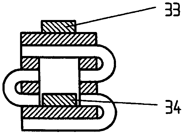
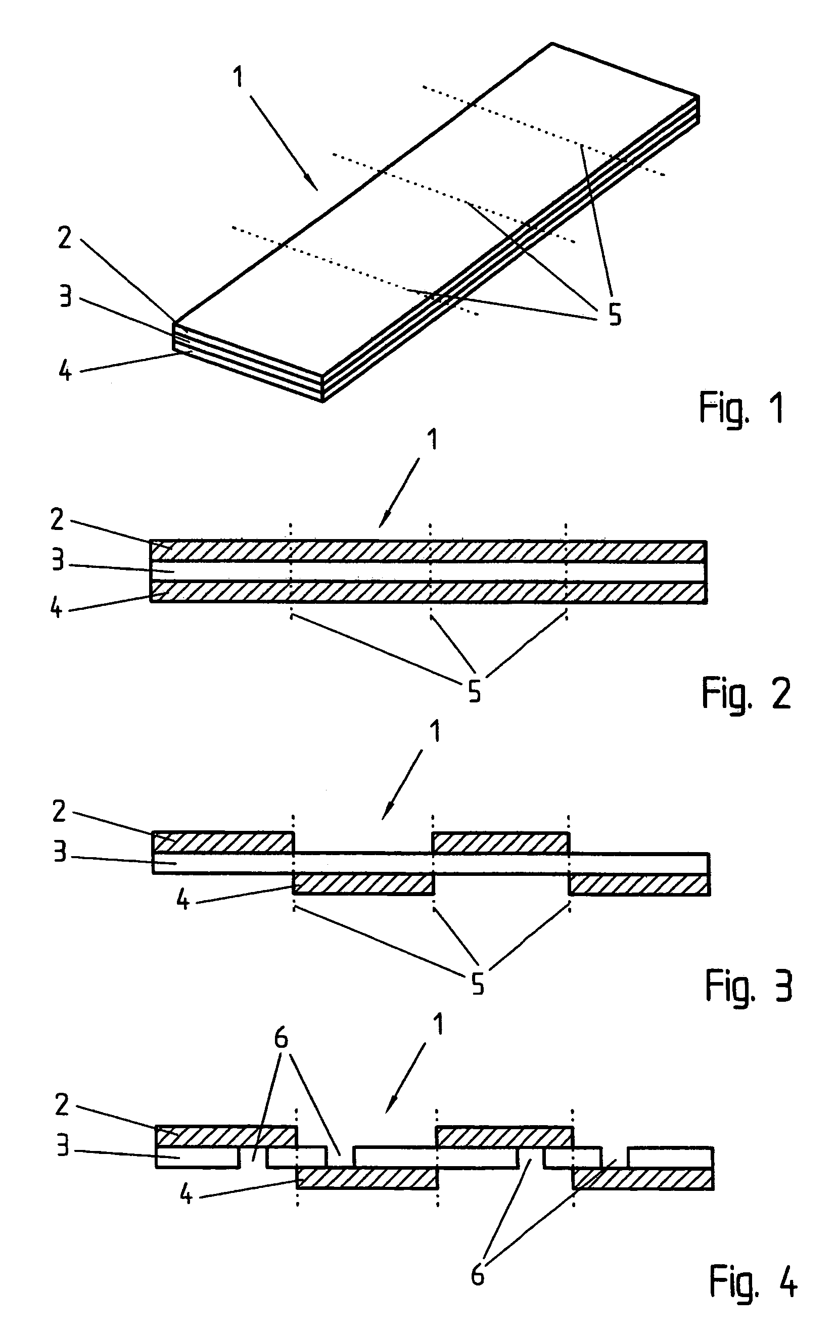
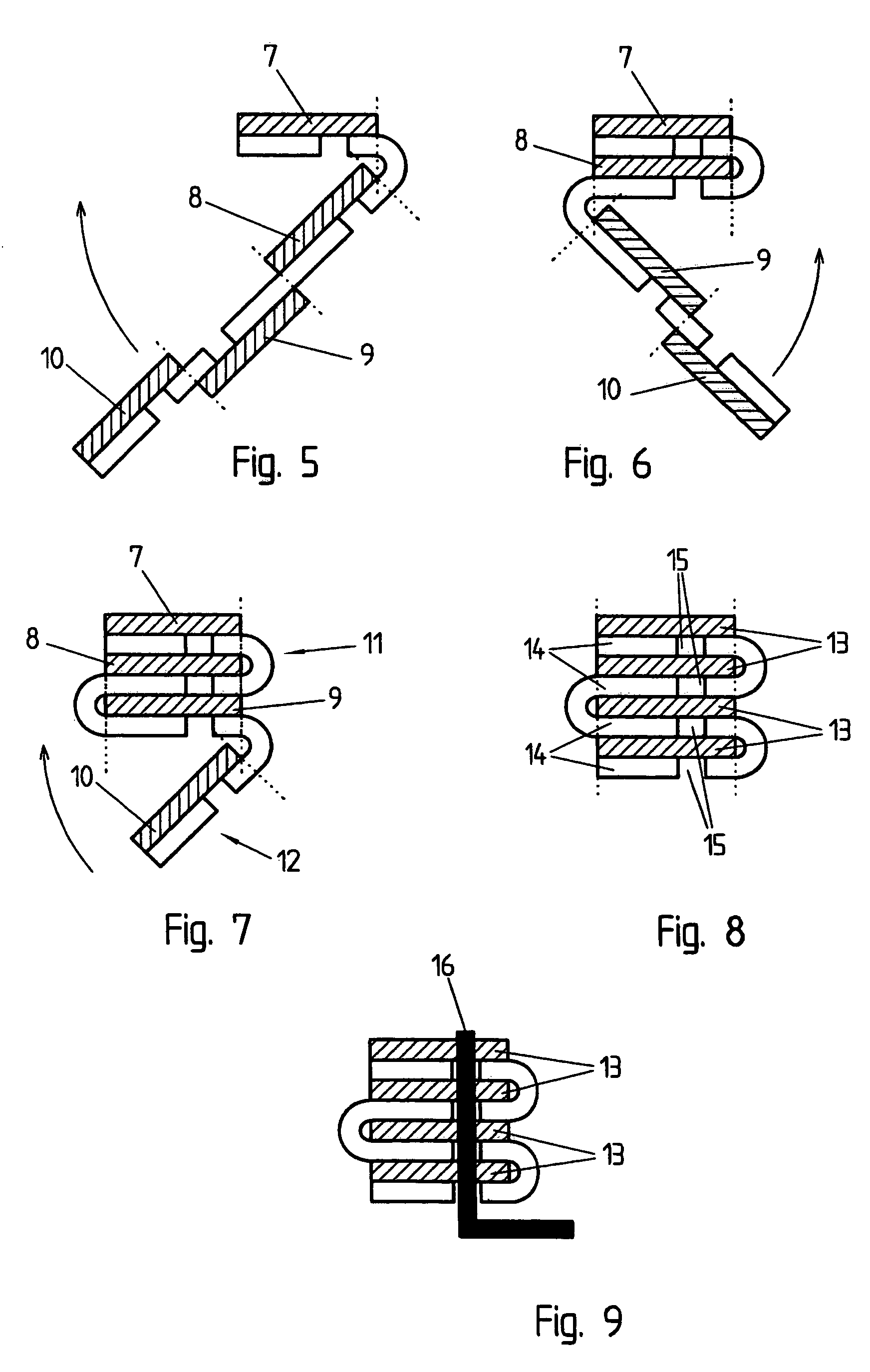
[0031]Reel-to-reel type processing is effective to use in manufacturing. The laminate is guided through the different process steps as a continuous strip. This eliminates many manual handling and alignment problems. Semi-finished products can also be stored and shipped between the various process steps in / on the reels. In FIG. 1, a projection of copper-kapton-copper laminate 1 (commonly called FLEX-laminate) is shown with copper 2, 4 and kapton 3 thicknesses of 75 μm and 25 μm, respectively. In FIG. 2, a cross section of such a laminate is also shown. Laminate like this is available on reels and its further processing is easy to automate. The intention is to process the laminate into the segments 5 which finally form the layers of the multilayer structure.

[0032]Processing begins as shown in FIG. 3 by forming the intended conductor pattern into two conductor layers 2 and 4 so that the conductor is alternately removed from the bottom and top sides of the insulator 3 from each segment....


PUM

PropertyMeasurementUnit
thicknessesaaaaaaaaaa
flexibleaaaaaaaaaa

Abstract

The invention relates to the manufacturing of a multilayer structure and especially it relates to the manufacturing of a three-dimensional structure and its use as an electronics assembly substrate and as a winding for transformers and inductors. When a multilayer structure is manufactured by folding a conductor-insulator-conductor laminate, where the conductor layers to be separated from each other follow each other on opposite sides of the conductor-insulator-conductor laminate in the sections following each other and where the insulator has been removed from the places where the conductor layers are to be connected together after folding, it is possible to manufacture a wide range of three-dimensional multilayer structures where the volume occupied by the windings over the total volume can be maximized. Alternatively, by using the method it is also possible to manufacture a multilayer structure where components have been buried inside. The method makes it also possible to make connections between layers in a flexible manner. Among other issues, the method can be easily automated for mass-production.

Description

REFERENCE DATA[0001]This application is a continuation of application PCT / EP02 / 11839 (WO03 / 036664), filed on Oct. 23, 2002, claiming priority of application FI20012052 of Oct. 23, 2001, the contents of which are hereby incorporated by reference.FIELD OF THE INVENTION[0002]The invention relates to the manufacturing of a multilayer structure and in particular to the manufacturing of a three dimensional structure and its use as an electronics assembly substrate and as a winding for transformers and inductors.DESCRIPTION OF RELATED ART[0003]Printed circuit boards are often used in electronics as substrate and to form electrical connections between components. Most commonly such circuit boards are manufactured by etching the preferred conductor pattern on a copper-insulator (copper-FR4) laminate and by drilling holes and through-plating them in order to form electrical connections from one side of the circuit board to the other. Multilayer printed circuit boards are manufactured by stack...

Claims


Application Information

Patent Timeline
Patent Type & Authority Patents(United States)
IPC IPC(8): H01L23/12H05K3/46H01F17/00H01F27/28H01F41/04H05K1/11H05K1/16H05K3/40
CPCH01F17/0013H01F41/041H05K1/118H05K3/4084H01F27/2804H01F27/2847H01F2027/2861H05K1/165H05K3/4092H05K2201/0379H05K2201/0394H05K2201/0397H05K2201/055H05K3/46
Inventor SIPPOLA, MIKA
Owner SCHAFFNER EMV AG
Why Eureka
Try Eureka