

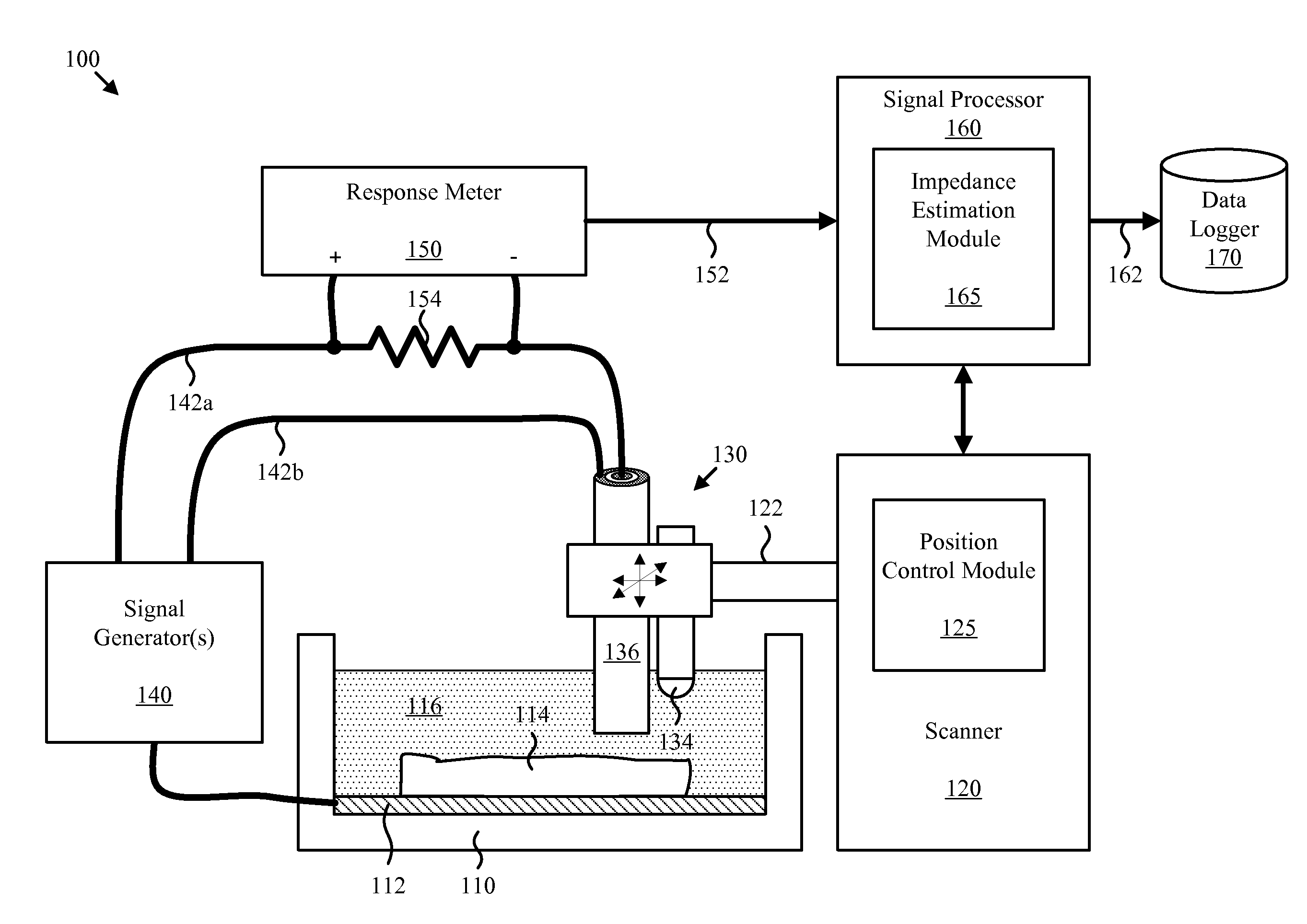
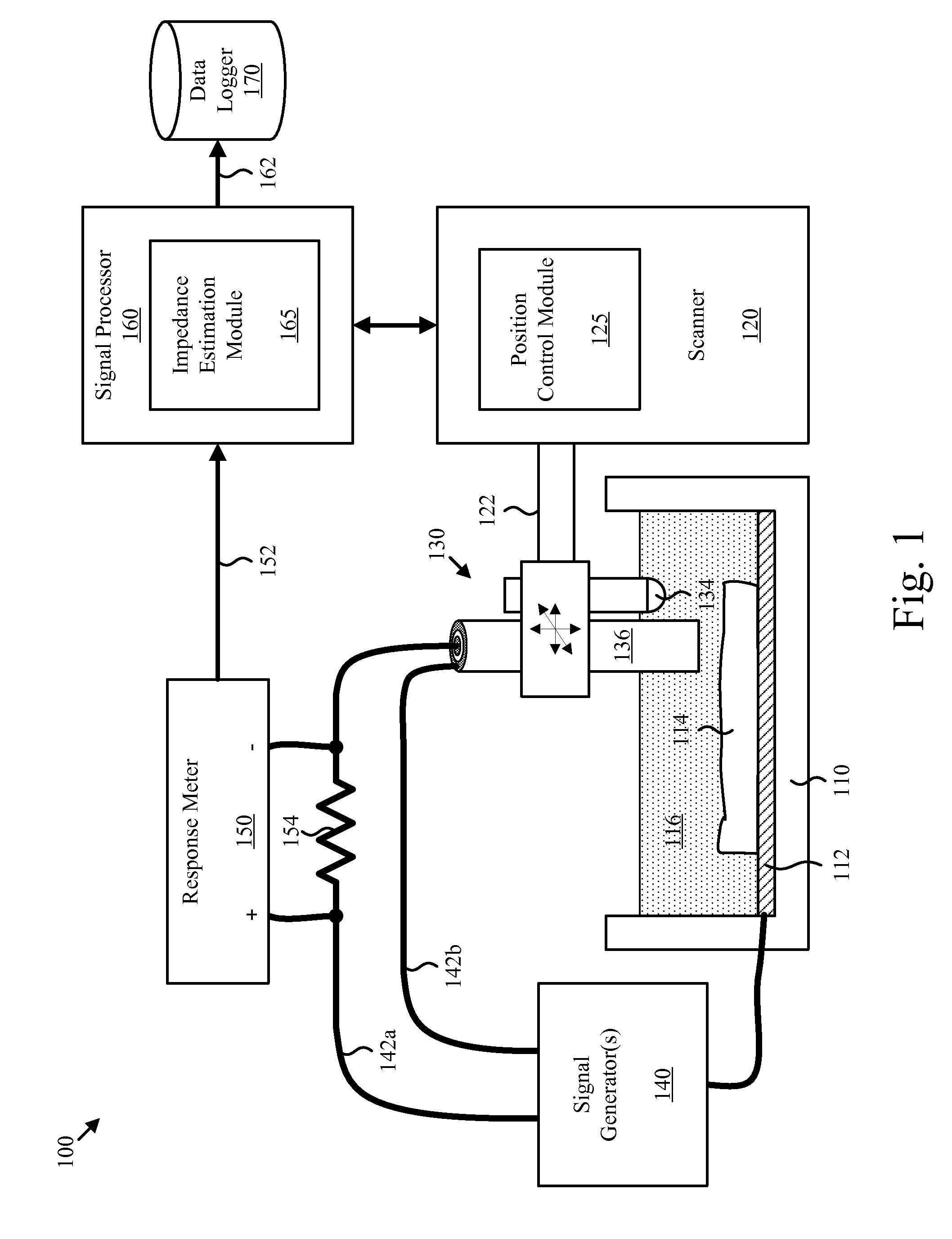
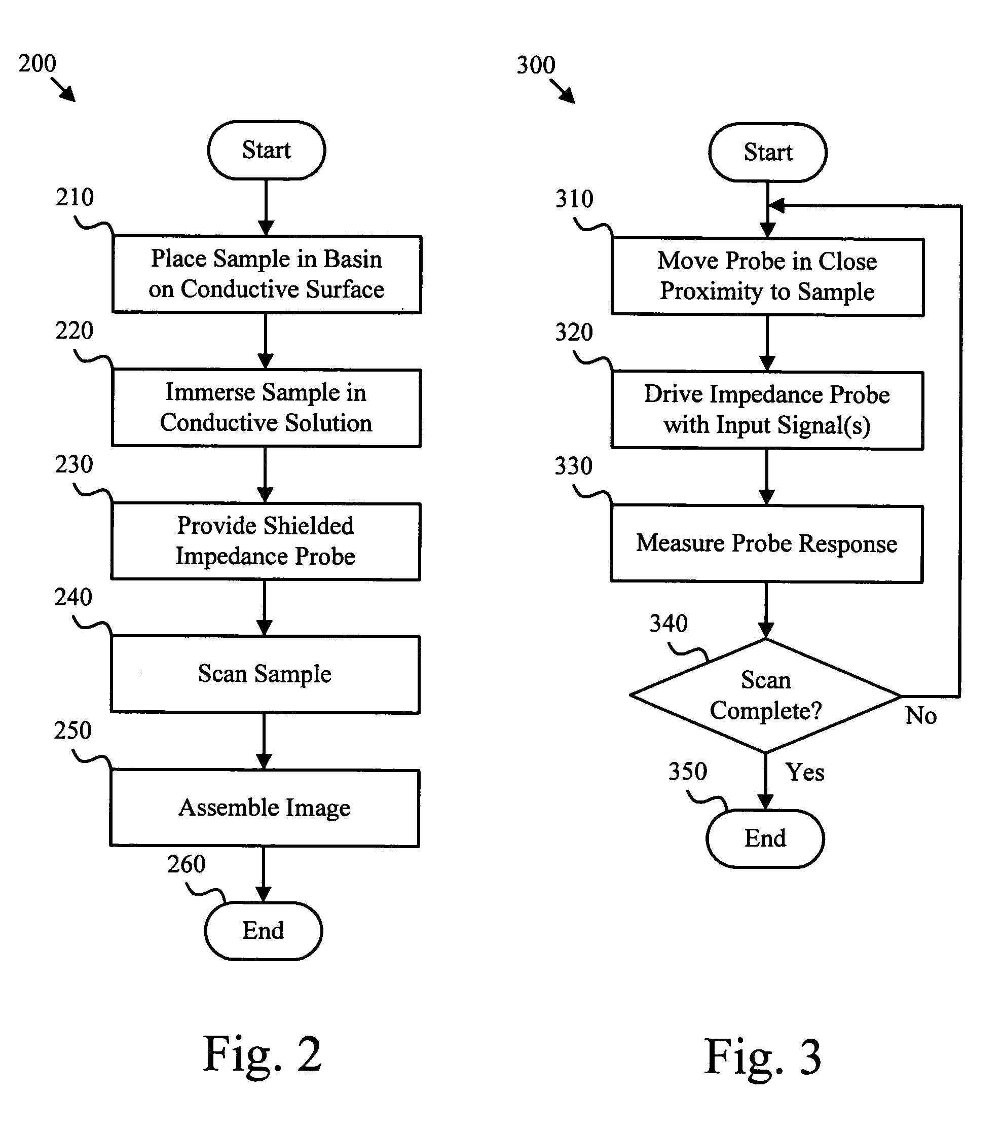
Scanned impedance imaging system method and apparatus
a scanning impedance and imaging system technology, applied in the field of scanning impedance scanning and imaging systems, can solve the problems of limiting the usefulness the resolution of electrical impedance tomography is very low, and the method is typically limited to providing surface profiles of scanned matter, so as to improve the directionality of electrical flux and measurement resolution.
- Summary
- Abstract
- Description
- Claims
- Application Information
AI Technical Summary
Benefits of technology
Problems solved by technology
Method used
Image

Examples
Embodiment Construction
[0033]Some of the functional units described in this specification have been explicitly labeled as modules, (while others are assumed to be modules) in order to emphasize their implementation independence. For example, a module may be implemented as a hardware circuit comprising custom VLSI circuits or gate arrays, off-the-shelf semiconductors such as logic chips, transistors, or other discrete components. A module may also be implemented in programmable hardware devices such as field programmable gate arrays, programmable array logic, programmable logic devices or the like.
[0034]Modules may also be implemented in software for execution by various types of processors. An identified module of executable code may, for instance, comprise one or more physical or logical blocks of computer instructions which may, for instance, be organized as an object, procedure, or function. Nevertheless, the executables of an identified module need not be physically located together, but may comprise ...
PUM
 Abstract
Description
Claims
Application Information