Calculating etch proximity-correction using image-precision techniques

a technology of image-precision and proximity correction, applied in the field of etch proximity correction, can solve the problems of inability to accurately capture the passivation effect, existing opc models do not calculate etch proximity correction accurately, and the proportion of instruments is increasing

Active Publication Date: 2007-04-17
SYNOPSYS INC
View PDF7 Cites 9 Cited by
  • Summary
  • Abstract
  • Description
  • Claims
  • Application Information

AI Technical Summary

Benefits of technology

[0015]In a variation on this embodiment, the statistical function, ƒ, is defined as ƒ(r,θ)=a / r, where r is a radial distance from the target point, θ is the angle between a cast ray and a reference line that passes through the target point, and a is a free parameter that is chosen so that a surface integral of the statistical function accurately models the amount of etch bias at the target point.

Problems solved by technology

As this miniaturization process causes features on integrated circuits to become progressively smaller, post-lithographic process effects are accounting for an ever-increasing portion of the CD (Critical Dimension) error budget.
Unfortunately, existing OPC models do not calculate etch proximity-correction accurately.
This cannot capture the passivation effect accurately because polygons that are not visible from the target point do not contribute to the proximity effect.
Linear convolution techniques cannot distinguish between visible and occluded polygons in every case.
As a result, in existing OPC models, the calculated etch proximity-correction lack much of the polygon orientation and the relative placement information needed for modeling of etch proximity.
This is the main reason why existing OPC models do not calculate etch proximity-correction accurately.

Method used


Image

  • Calculating etch proximity-correction using image-precision techniques
  • Calculating etch proximity-correction using image-precision techniques
  • Calculating etch proximity-correction using image-precision techniques

Examples


Embodiment Construction

Optical Proximity Correction (OPC)

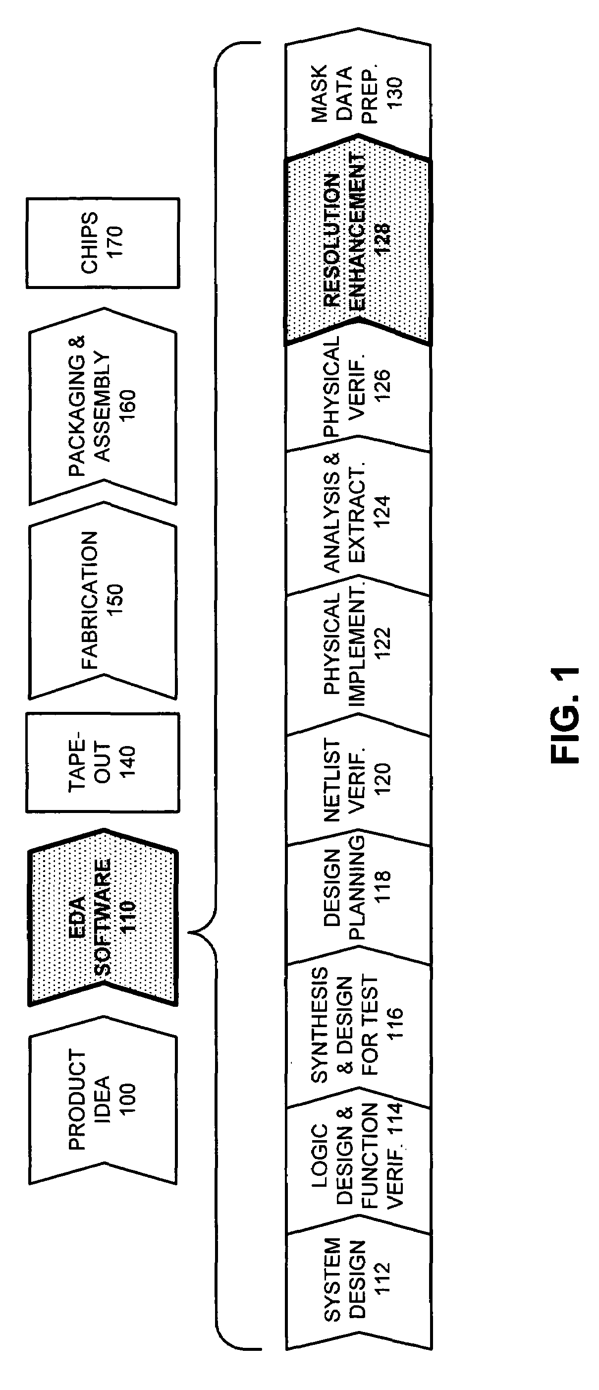
[0023]FIG. 1 illustrates the various steps in the design and fabrication of an integrated circuit in accordance with an embodiment of the present invention. The process starts with a product idea (step 100). Next, the product idea is realized by an integrated circuit, which designed using Electronic Design Automation (EDA) software (step 110). Once the design is finalized in software, it is taped-out (step 140). After tape-out, the process goes through fabrication (step 150), packaging, and assembly (step 160). The process eventually culminates with the production of chips (step 170).

[0024]The EDA software design step 110, in turn, includes a number of sub-steps, namely, system design (step 112), logic design and function verification (step 114), synthesis and design for test (step 116), design planning (step 118), netlist verification (step 120), physical implementation (step 122), analysis and extraction (step 124), physical verification (step 126...


PUM


Abstract

One embodiment of the present invention provides a system that calculates etch proximity-correction during an OPC (Optical Proximity Correction) process. During operation, the system receives a layout for an integrated circuit. Next, the system selects a target point on an edge in the layout. The system then casts a plurality of rays from the target point, and constructs a plurality of pie-wedges based on the cast rays. The system then computes a surface integral of a statistical function over the pie-wedges, wherein the surface integral of the statistical function models the etch bias at the target point. Next, the calculated etch proximity-correction is applied to an area in proximity to the target point.

Description

RELATED APPLICATIONS[0001]The subject matter of this application is related to the subject matter in a non-provisional application by the same inventors as the instant application and filed on the same day as the instant application entitled, “CALCULATING ETCH PROXIMITY-CORRECTION USING OBJECT-PRECISION TECHNIQUES,” having Ser. No. 10 / 955,532, and filing date Sep. 29, 2004.BACKGROUND[0002]1. Field of the Invention[0003]This invention relates to the process of fabricating semiconductor chips. More specifically, the invention relates to a method and apparatus for calculating etch proximity-correction during the OPC (Optical Proximity Correction) process.[0004]2. Related Art[0005]The relentless miniaturization of integrated circuits has been a key driving force behind recent advances in computer technology. As this miniaturization process causes features on integrated circuits to become progressively smaller, post-lithographic process effects are accounting for an ever-increasing porti...

Claims


Application Information

Patent Timeline
Patent Type & Authority Patents(United States)
IPC IPC(8): G06F17/50
CPCG03F1/144G03F1/36G03F1/80
Inventor BEALE, DANSHIELY, JIMSTIRNIMAN, JOHN
Owner SYNOPSYS INC
Why Eureka
Try Eureka