Light sensing panel, and liquid crystal display apparatus having the same

a technology of light sensing panel and liquid crystal display device, which is applied in the direction of static indicating device, optical radiation measurement, instruments, etc., can solve the problems of insufficient size of the region in which the light sensing sensor is disposed, increased possibility of defects, and limited design of array substrate, etc., to achieve a reduced electrical coupling between devices, enhance display quality, and reduce the effect of aperture ratio

Active Publication Date: 2007-04-24
SAMSUNG DISPLAY CO LTD
View PDF1 Cites 25 Cited by
  • Summary
  • Abstract
  • Description
  • Claims
  • Application Information

AI Technical Summary

Benefits of technology

[0015]The present invention provides a light sensing panel having a light sensing sensor with simple structure in order to reduce lowering of aperture ratio, defects and interference.
[0020]According to the present invention, the light sensing panel requires only one thin film transistor in order to detect a position wherein the external light is incident. Therefore, electrical coupling between devices is reduced and aperture ratio is increased, thereby enhancing a display quality.

Problems solved by technology

However, a size of a region in which the light sensing sensor is disposed is insufficient.
Therefore, a design for the array substrate may be limited.
Therefore, possibility of defects may increase.
Furthermore, possibility of interference between the devices may also increase.

Method used


Image

  • Light sensing panel, and liquid crystal display apparatus having the same
  • Light sensing panel, and liquid crystal display apparatus having the same
  • Light sensing panel, and liquid crystal display apparatus having the same

Examples


Embodiment Construction

[0030]Hereinafter, the embodiments of the present invention will be described in detail with reference to the accompanied drawings.

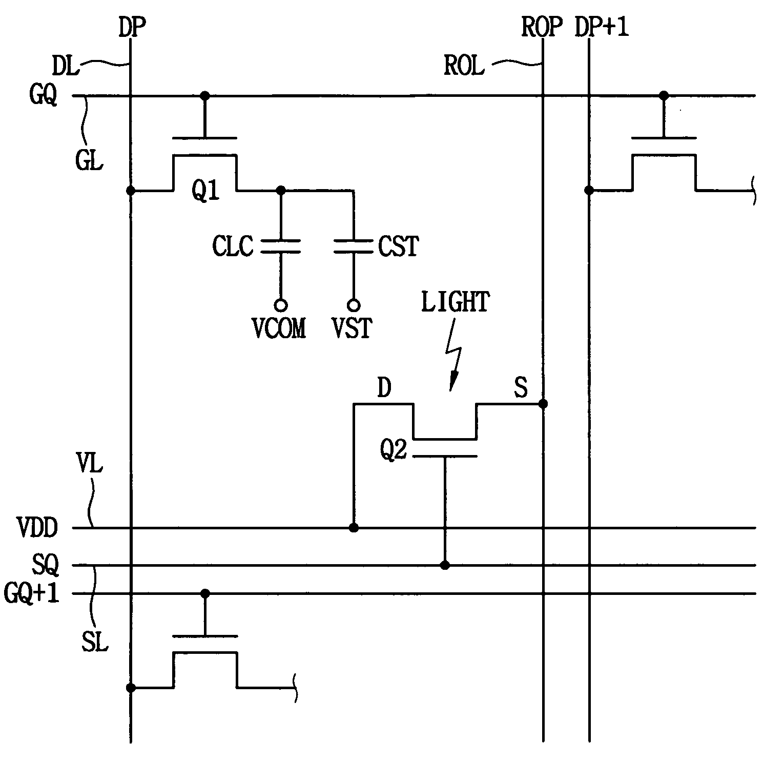
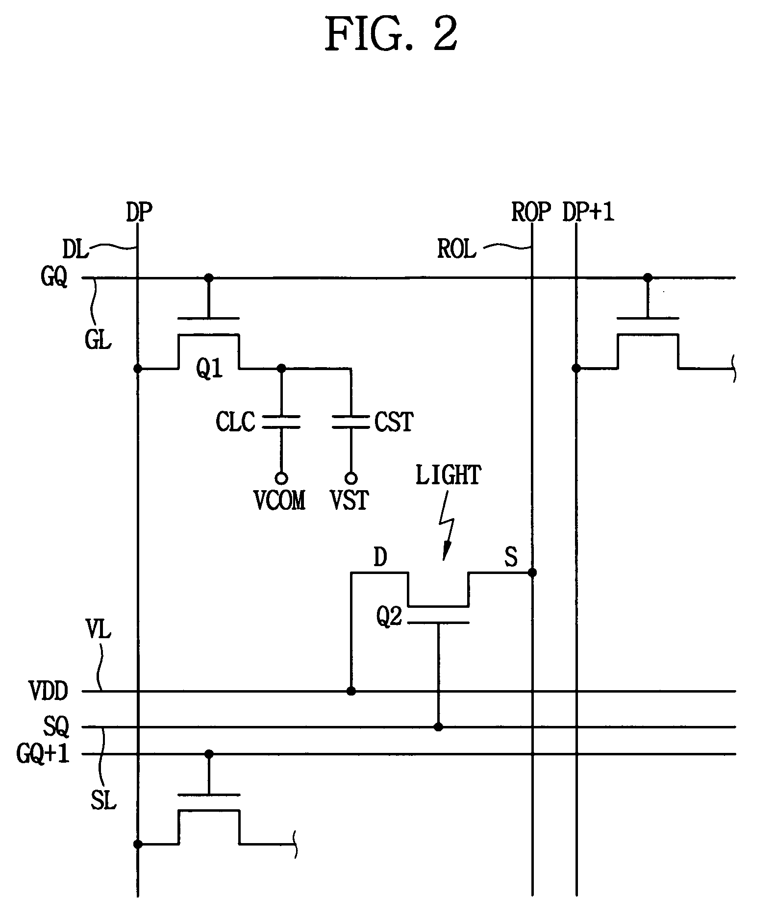
[0031]FIG. 2 is an equivalent circuit diagram of a light sensing sensor according to an exemplary embodiment of the present invention. FIG. 2 illustrates only one unit pixel of a liquid crystal display panel.

[0032]Referring to FIG. 2, a liquid crystal display panel having a light sensing sensor includes a gate line GL, a data line DL, a switching device Q1, a liquid crystal capacitor CLC, a storage capacitor CST, a power source line VL, a scan line SL, a light sensing device Q2 and a readout line ROL.

[0033]The gate line GL is extended in a horizontal direction, and a gate signal GQ is applied to the switching device Q1 via the gate line GL. The data line DL is extended in a vertical direction, and a data signal DP is applied to the switching device Q1.

[0034]The switching device Q1 is formed in a region defined by the gate line GL and the data line DL. Th...


PUM

PropertyMeasurementUnit
bias voltageaaaaaaaaaa
bias voltage VDDaaaaaaaaaa
voltageaaaaaaaaaa

Abstract

A light sensing panel includes a scan line transmitting a scan signal, a power source line transmitting a bias voltage, a readout line transmitting a light sensing signal and a light sensing device. The light sensing device includes a control electrode that is electrically connected to the scan line to receive the scan signal, a first current electrode that is electrically connected to the power source line to receive the bias voltage, and a second current electrode that is electrically connected to the readout line to apply a light sensing signal to the readout line when the light sensing signal senses an external light. The light sensing panel requires only one thin film transistor in order to detect a position wherein the external light is incident. Therefore, electrical coupling between devices is reduced and aperture ratio is increased, thereby enhancing a display quality.

Description

CROSS-REFERENCE TO RELATED APPLICATIONS[0001]This application relies for priority upon Korean Patent Application No.2003-97144 filed on Dec. 26, 2003, the contents of which are herein incorporated by reference in its entirety.BACKGROUND OF THE INVENTION[0002]1. Field of the Invention[0003]The present invention relates to a light sensing panel and liquid crystal display apparatus having the light sensing panel. More particularly, the present invention relates to a light sensing panel that prevents lowering of aperture ratio, and a liquid crystal display apparatus having the light sensing panel.[0004]2. Description of the Related Art[0005]Generally, a light sensing sensor senses an external light to detect an entrance position of the external light. Willem den Boer disclosed a liquid crystal display apparatus having a plurality of the light sensing sensors arranged in a matrix shape to have a function of finger print identification or touch panel by a paper entitled “Active Matrix LCD...

Claims


Application Information

Patent Timeline
Patent Type & Authority Patents(United States)
IPC IPC(8): G01J1/44G01J1/42G02F1/136G02F1/13G02F1/133G02F1/1333G02F1/1362H01L21/77H01L21/84H01L27/00H01L27/12
CPCG02F1/1362H01L27/1214G02F2001/13312G02F1/13312G02F1/133
Inventor PARK, SANG-JINUH, KEE-HANJUNG, YOUNG-BAECHO, JONG-WHANCHOI, YOUNG-JUN
Owner SAMSUNG DISPLAY CO LTD
Why Eureka
Try Eureka