Method and system for sampling a signal

a signal sampling and signal technology, applied in the field of analog to digital conversion and digital to analog conversion, can solve the problems of affecting the performance of the rf front-end circuitry, generating high frequency interference, and significant detrimental noise and interference in the digital processing circuitry of a typical communication apparatus

Inactive Publication Date: 2007-04-24
SILICON LAB INC
View PDF68 Cites 21 Cited by
  • Summary
  • Abstract
  • Description
  • Claims
  • Application Information

AI Technical Summary

Problems solved by technology

Unfortunately, the digital processing circuitry of a typical communication apparatus can be a significant source of detrimental noise and interference.
As a result, they generate high frequency interference.
These spurious emissions may interfere with, and may adversely impact, the performance of the RF front-end circuitry.
However in certain implementations, integration of the RF front-end circuitry and digital processing circuitry on a single integrated circuit may present challenges due to digital noise from the digital processing circuitry.

Method used


Image

  • Method and system for sampling a signal
  • Method and system for sampling a signal
  • Method and system for sampling a signal

Examples


Embodiment Construction

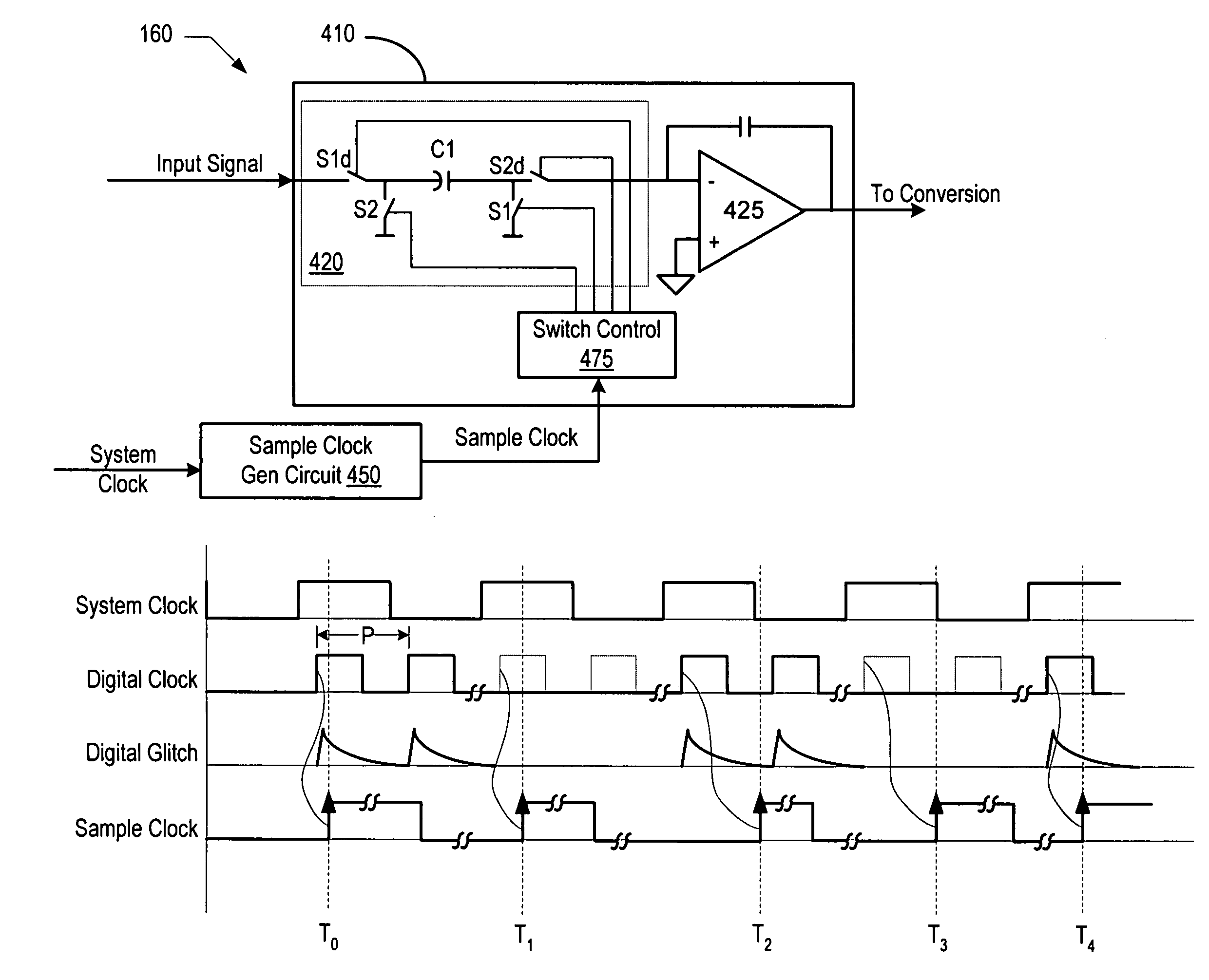
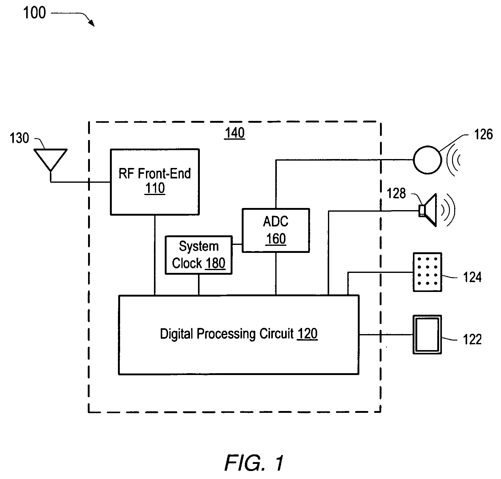
[0020]Turning now to FIG. 1, a generalized block diagram of a communication apparatus 100 including an RF front-end circuit 110 coupled to a digital processing circuit 120 is shown. As illustrated, various user interfaces including a display 122, a keypad 124, a microphone 126, and a speaker 128 may be coupled to digital processing circuit 120, depending upon the specific application of communication apparatus 100 and its desired functionality. An antenna 130 is also shown coupled to RF front-end circuit 110.

[0021]Communication apparatus 100 is illustrative of various wireless devices including, for example, mobile and cellular phone handsets, machine-to-machine (M2M) communication networks (e.g., wireless communications for vending machines), so-called “911 phones” (a mobile handset configured for calling the 911 emergency response service), as well as devices employed in emerging applications such as 3G, satellite communications, and the like. As such, communication apparatus 100 ...


PUM


Abstract

A system includes a digital circuit that may be clocked by a digital clock signal having an associated clock period. The system also includes a sample clock generation circuit coupled to a sampling circuit. The sample clock generation circuit may be configured to receive an input clock having a fixed phase relationship with respect to the digital clock signal. The sample clock generation circuit may also generate a sample clock having a first sampling edge corresponding to a first relative offset within the clock period and a subsequent sampling edge corresponding to a different relative offset within the clock period. The sampling circuit may be configured to sample a designated signal upon a first sampling instance corresponding to the first sampling edge and to sample the designated signal upon a subsequent sampling instance corresponding to the subsequent sampling edge.

Description

BACKGROUND OF THE INVENTION[0001]1. Field of the Invention[0002]This invention relates generally to analog to digital conversion and digital to analog conversion and, more particularly, to converting analog signals to digital representations in the presence of digital noise.[0003]2. Description of the Related Art[0004]High performance wireless communication apparatus such as RF receivers, transmitters, and transceivers typically include RF front-end circuitry that operates on an RF signal being received or transmitted. For example, the front-end circuitry may down-convert a received RF signal to baseband and / or up-convert a baseband signal for RF transmission. The RF front-end circuitry typically includes analog circuits such as low noise amplifiers and mixers that have a relatively high sensitivity to noise and interference. The RF circuitry in some applications, such as in mobile communication cellular handsets, may be required to detect signals as small as a few micro-volts or le...

Claims


Application Information

Patent Timeline
Patent Type & Authority Patents(United States)
IPC IPC(8): H03M1/00
CPCH03M1/0658H03M1/128H03M3/336H03M1/0818H03M1/1215H03M3/47H03M3/458H03M3/3283
Inventor SOMAYAJULA, SHYAM S.
Owner SILICON LAB INC
Why Eureka
Try Eureka