Bonding pad structure for a display device and fabrication method thereof
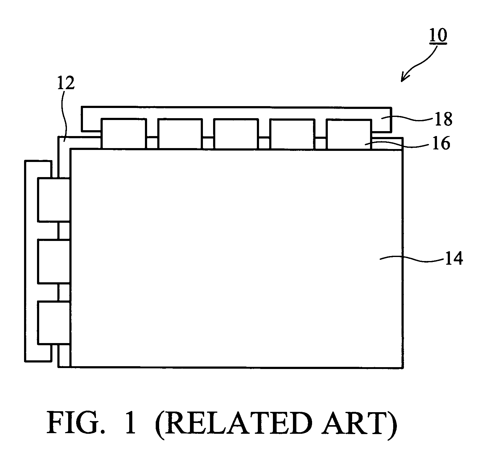
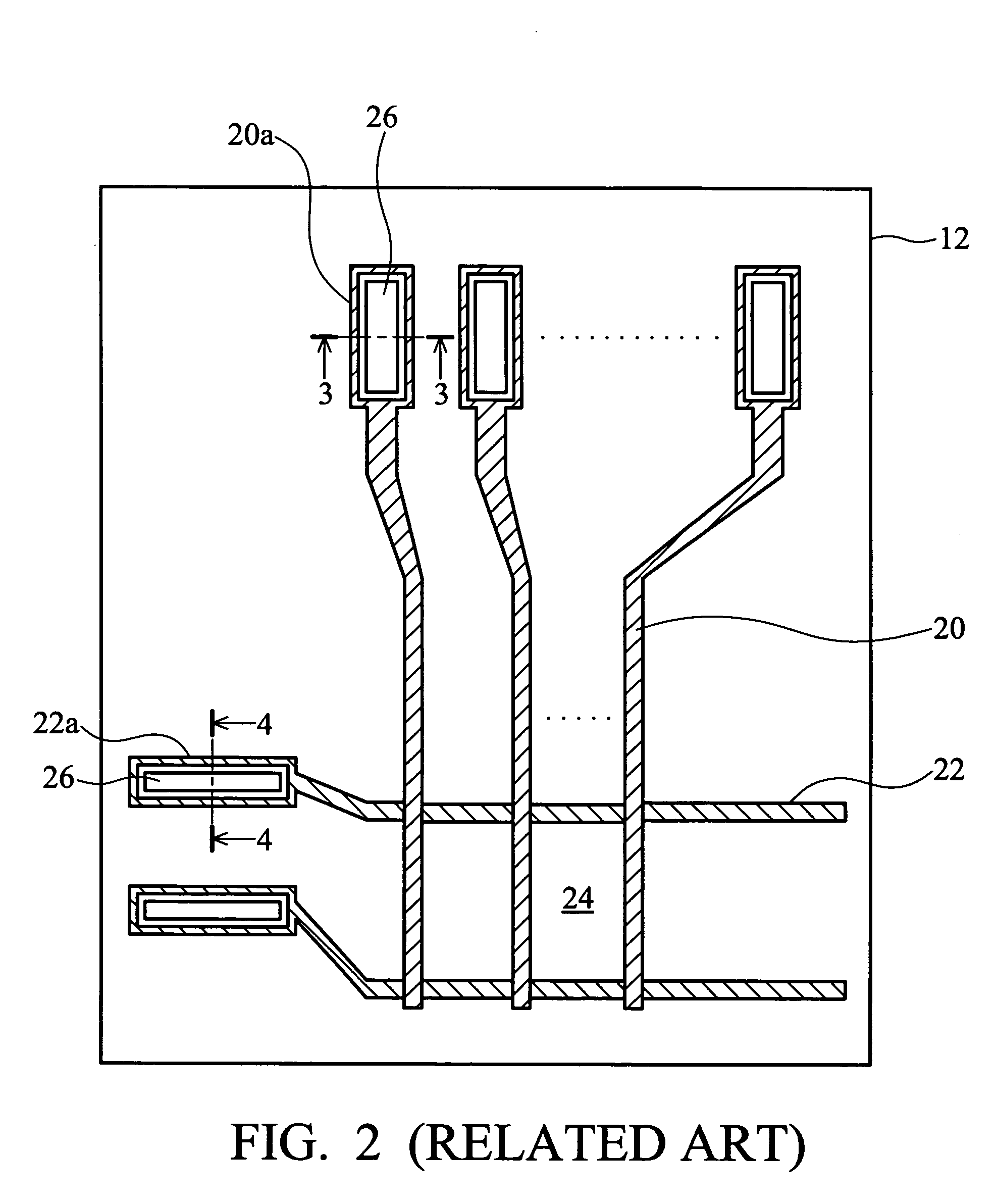
a technology of display device and bonding pad, which is applied in the direction of electrical apparatus construction details, printed circuit non-printed electric components association, instruments, etc., can solve the problems of poor reliability, metal layer scratching, and product defects
- Summary
- Abstract
- Description
- Claims
- Application Information
AI Technical Summary
Benefits of technology
Problems solved by technology
Method used
Image
Examples
first embodiment
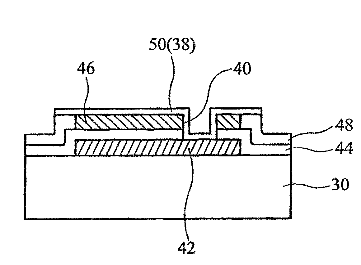
[0026]FIG. 6 is a plane view of a bonding pad structure according to the first embodiment of the present invention. A display substrate 30 comprises a plurality of scanning lines 32 extending along a first direction and a plurality of data lines 34 extending along a second direction, which intersect to define an array of pixel areas 36. Each pixel area 36 comprises a switching device (such as a TFT device) and a pixel electrode. Each scanning line 32 has a terminal portion on which a bonding pad 38 is formed and electrically connected to an external IC board through a signal processing substrate. Similarly, each data line 34 has a terminal portion on which a bonding pad 38 is formed and electrically connected to an external IC board through a signal processing substrate. In addition, an opening structure 40 is designed beneath each bonding pad 38 to make the bonding pad 38 contact two conductive layers simultaneously, resulting in two electrical-connection paths.
[0027]FIG. 7 is a cr...
second embodiment
[0030]The bonding pad structure and the fabrication method thereof in the second embodiment are substantially similar to those of the first embodiment, and similar portions omitted herein. The different portion is the profile and number of the opening structure 40. In each bonding pad structure of the first embodiment, the opening structure 40 is one via. In each bonding pad structure of the second embodiment, the opening structure 40 may be a plurality of vias, a strip trench or a circuit trench.
[0031]FIGS. 9, 10 and 11A are plane views illustrating examples of bonding pad structures according to the second embodiment of the present invention. FIG. 11B is a cross-section along line 11—11 of FIG. 11A illustrating the bonding pad structure according to the second embodiment of the present invention.
[0032]In FIG. 9, each opening structure 40 comprises at least two vias, and the diameter, symmetry and arrangement of the vias are not limited.
[0033]In FIG. 10, each opening structure 40 c...
PUM
| Property | Measurement | Unit |
|---|---|---|
| conductive | aaaaa | aaaaa |
| structure | aaaaa | aaaaa |
| transparent | aaaaa | aaaaa |
Abstract
Description
Claims
Application Information


