Driver for driving a load using a charge pump circuit

a charge pump and load technology, applied in the direction of electrical devices, devices without intermediate ac conversion, semiconductor devices, etc., can solve the problems of insufficient charging voltage, constant voltage change, and variable capacitance of the load driver, so as to greatly improve the step-up performance of the charge pump circuit

Inactive Publication Date: 2007-05-08
ROHM CO LTD
View PDF6 Cites 5 Cited by
  • Summary
  • Abstract
  • Description
  • Claims
  • Application Information

AI Technical Summary

Benefits of technology

[0031]A MOS capacitor of the invention can be used effectively in a charge pump circuit, especially in the first stage where the voltage dependent characteristic is significant

Problems solved by technology

The magnitudes of these capacitances are not very large that they may not be sufficient for building up the required charging voltage when the power consumed by the load 12 is large.
Unfortunately, the MOS capacitors as shown in FIGS. 2 and 3 have a disadvantageous characteristic (hereinafter referred to as voltage dependent characteristic) that their capacitances vary with the voltages applied thereto.
However, a MOS capacitor for a charge pump circuit is subjected to frequent charging and discharging, and hence its voltage is always changing.
Particularly, the voltage impressed on the first stage MOS capacitor is low and th

Method used


Image

  • Driver for driving a load using a charge pump circuit
  • Driver for driving a load using a charge pump circuit
  • Driver for driving a load using a charge pump circuit

Examples


Embodiment Construction

[0042]The invention will now be described in detail by way of example with reference to the accompanying drawings.

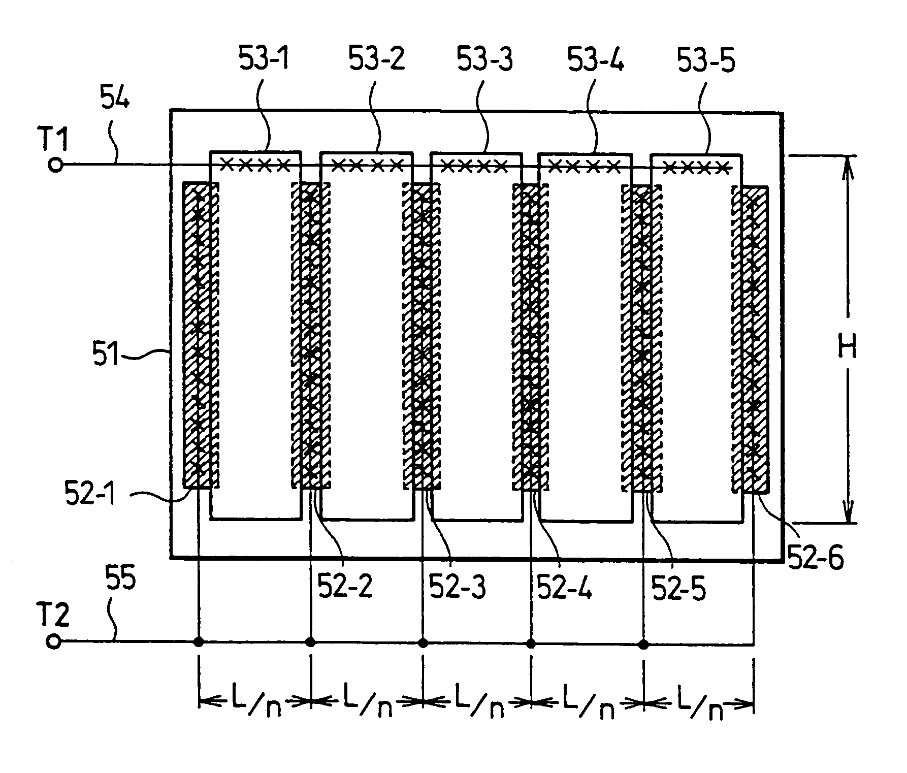
[0043]Referring to FIGS. 5 and 6, there is shown a MOS capacitor of one embodiment of the invention, used in a charge pump circuit formed together with other elements such as MOSFETs on the same semiconductor substrate of a semiconductor apparatus. Particularly, FIGS. 5 and 6 schematically show the top view and the cross sectional view, respectively, of the MOS capacitor of the invention.

[0044]FIG. 7 shows an equivalent circuit of a MOS capacitor, representing the operation of the MOS capacitor. FIG. 8 compares voltage-capacitance characteristic of an inventive MOS capacitor with that of a conventional MOS capacitor.

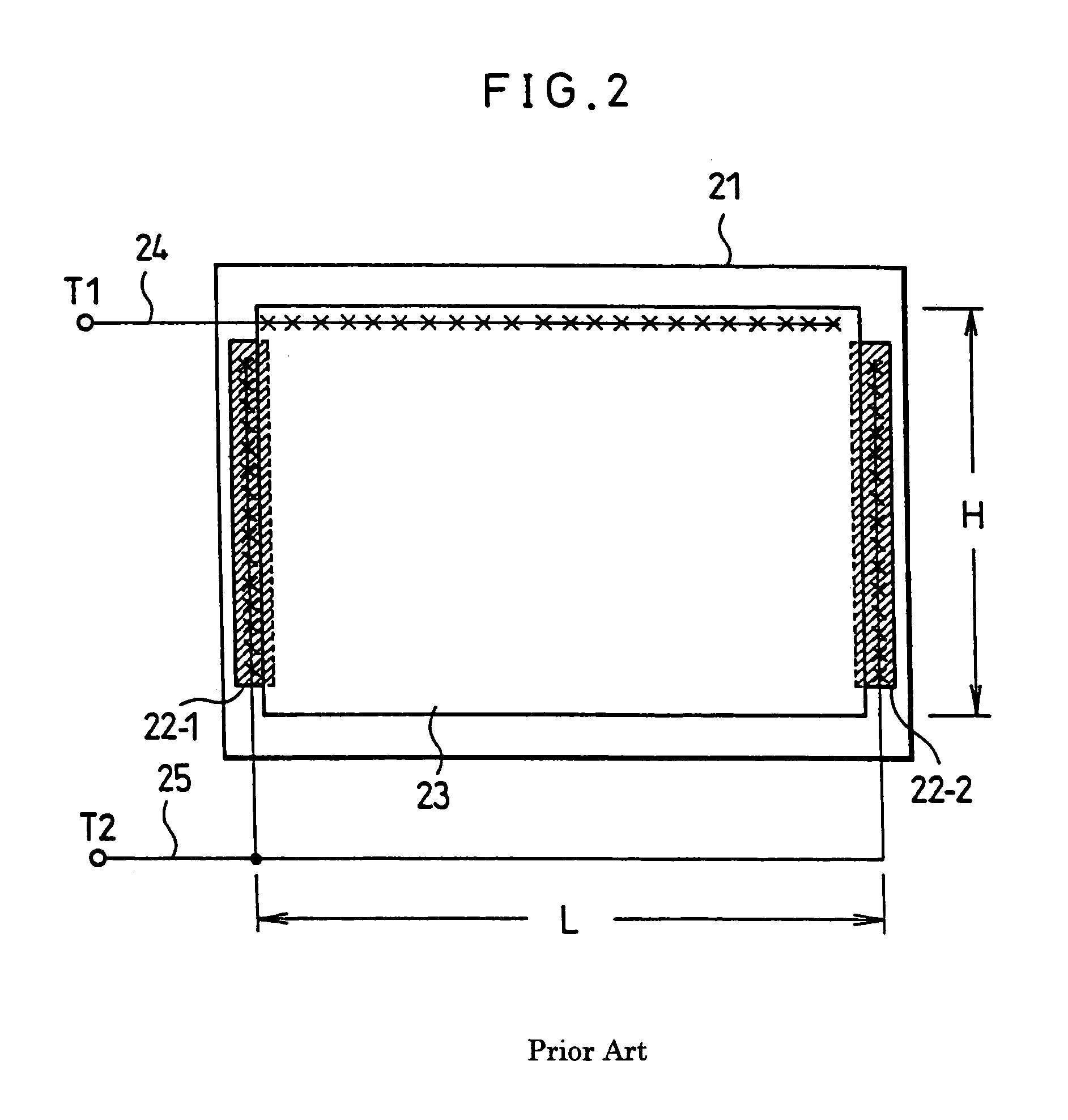
[0045]As shown in FIGS. 5 and 6, an N-well region 51 is formed on a p-type substrate 50. The N-well region 51 is surrounded by isolation regions in the form of, for example, oxide layers 58-1 and 58-2 to electrically isolate the MOS capacitor from other eleme...


PUM


Abstract

A charge pump circuit includes MOSFETs and MOS capacitors formed on the same substrate. Each of the MOS capacitors has a multiplicity of first electrodes formed in one region of the substrate, insulating layers formed on/above respective substrate regions between neighboring first electrodes, each layer covering at least the respective substrate region, and a multiplicity of second electrodes formed on/above the respective insulating layers. The MOS capacitors have improved frequency response.

Description

[0001]This is a continuation of application Ser. No. 09 / 991,307 filed Nov. 13, 2001 now U.S. Pat. No. 6,693,316, which application is hereby incorporated by reference in its entirety.FIELD OF THE INVENTION[0002]The invention relates to a semiconductor apparatus having a charge pump circuit, and more particularly to a semiconductor apparatus having a charge pump circuit which includes MOS type charge pump capacitors.BACKGROUND OF THE INVENTION[0003]Semiconductor apparatuses such as an LCD driver which has a low-voltage logic and a high-voltage logic on the same semiconductor chip are designed to generate a high voltage by stepping up a low-voltage of a low voltage supply using a charge pump circuit.[0004]FIG. 1 illustrates such a charge pump circuit 11, in which a high voltage Vo (15 V) is obtained for a load 12 by stepping up a low voltage supply Vcc (about 3 V) of the power supply 13. As shown in FIG. 1, the charge pump circuit 11 has: p-type MOSFETs Q1–Qn connected in series betwe...

Claims


Application Information

Patent Timeline
IPC IPC(8): H01L29/00H01L27/04H01L21/822H01L21/8234H01L27/02H01L27/06H01L27/08
CPCH01L27/0222H01L27/0805H01L29/41758H02M3/07
Inventor TANAKA, TOSHIMASAOKU, HIRONORI
Owner ROHM CO LTD
Why Eureka
Try Eureka