

Plasma display apparatus and fluorescent material for plasma display panel
a technology of plasma display panel and fluorescent material, which is applied in the direction of discharge tube/lamp details, discharge tube luminescnet screen, gas-filled discharge tube, etc., can solve the problems of unsatisfactory uniformity in displaying images in a display region, unsatisfactory display region, and unsatisfactory display region. achieve the effect of preventing a local increase in voltag
- Summary
- Abstract
- Description
- Claims
- Application Information
AI Technical Summary
Benefits of technology
Problems solved by technology
Method used
Image

Examples
first embodiment
[First Embodiment]
[0054]The fluorescent material in accordance with the first embodiment emits green light.
[0055]As fluorescent material which emits green light, there may be selected Zn2SiO4:Mn, (Y, Gd)BO3:Tb or YBO3:Tb, for instance.
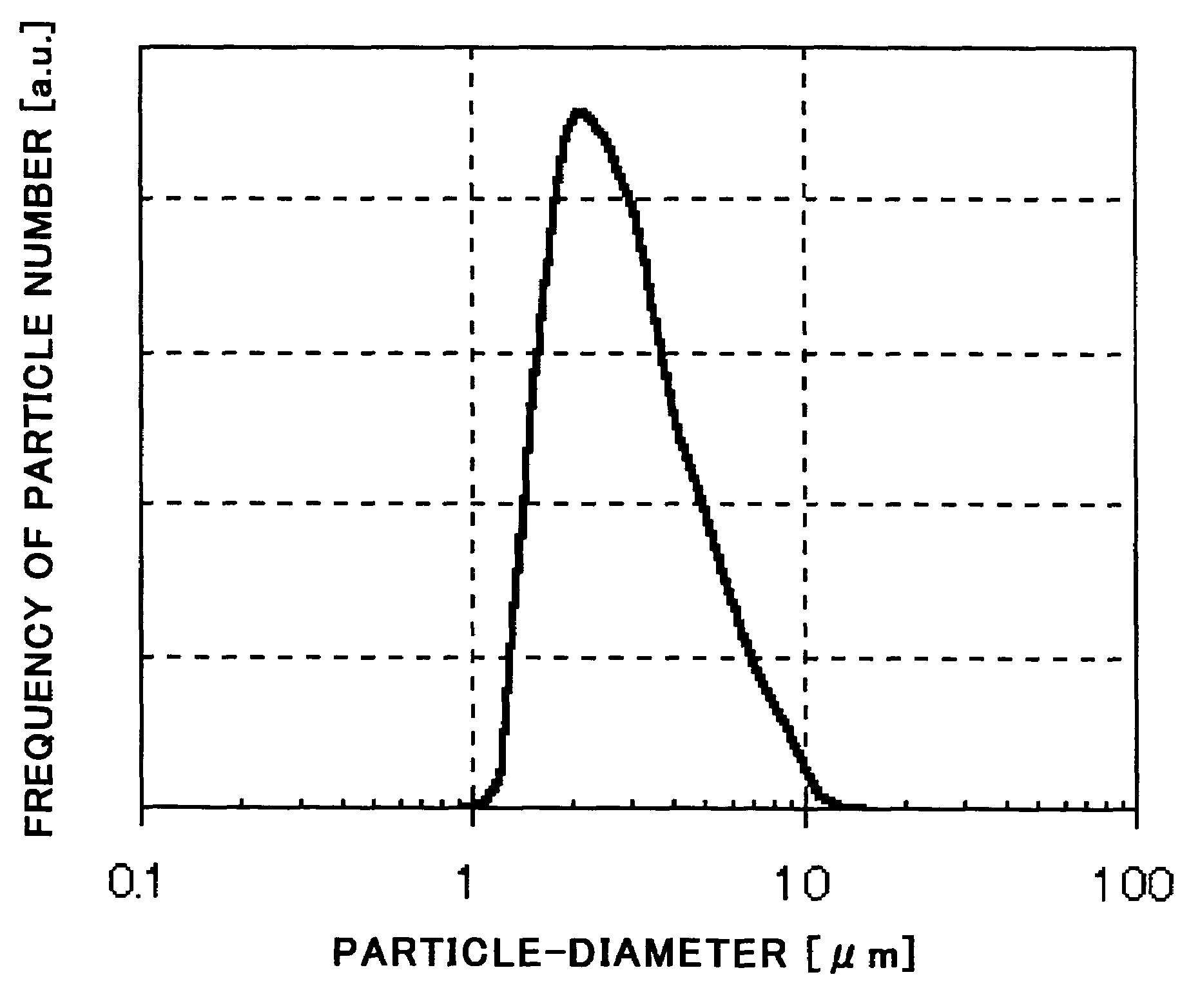
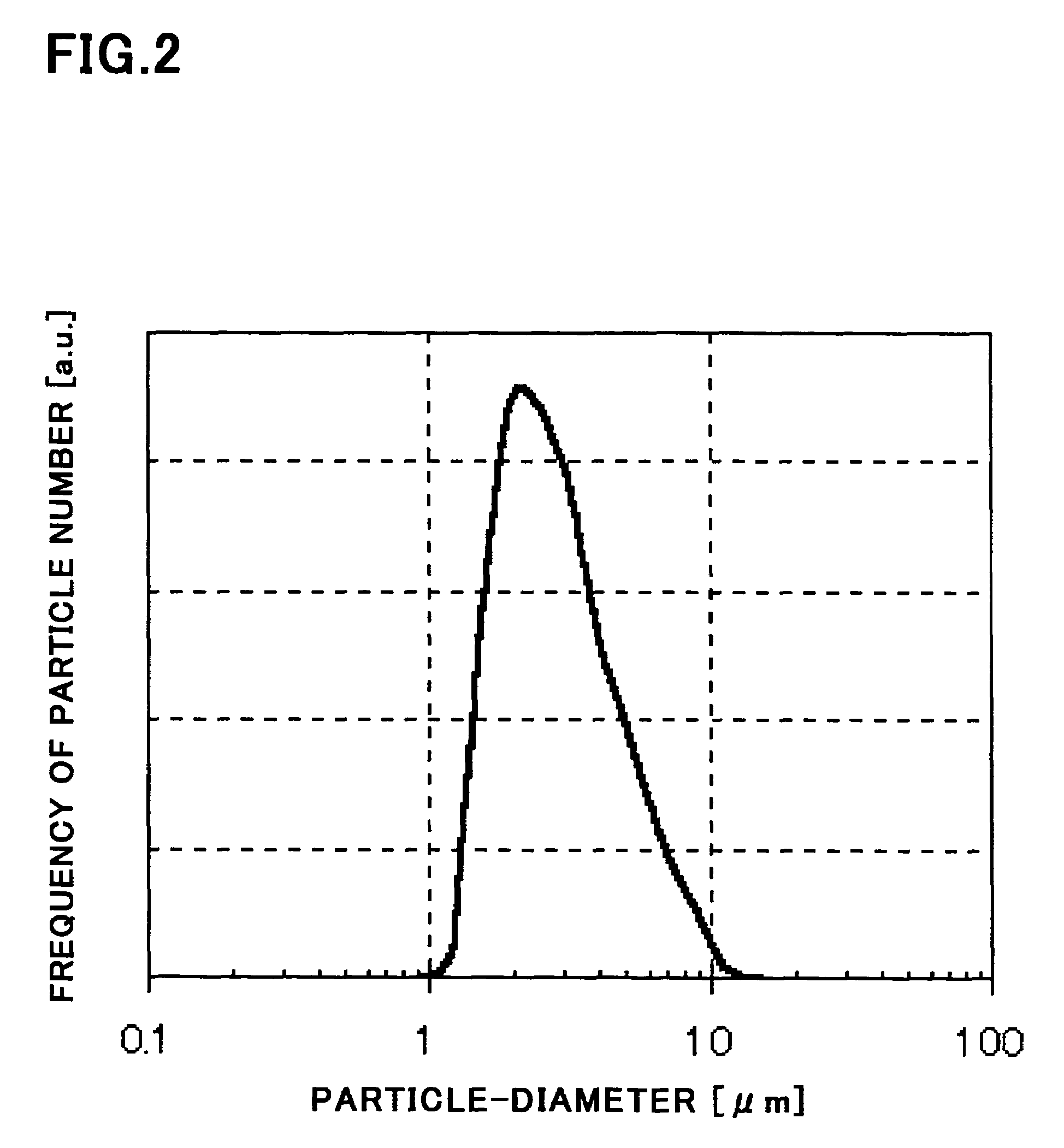
[0056]FIG. 2 is a histogram showing a particle-diameter profile of the fluorescent material in accordance with the first embodiment of the present invention, and FIG. 3 is a histogram showing a particle-diameter profile of conventional fluorescent material from which green light emits. In FIGS. 2 and 3, the axis of abscissa indicates a particle diameter in a unit of micrometer [μm], and the axis of ordinates indicates a frequency of a number of particles in an arbitrary unit [a.u.].
[0057]As is obvious in comparison of FIGS. 2 and 3 with each other, a particle-diameter profile of the fluorescent material in accordance with the first embodiment is narrower than the same of conventional fluorescent material.
[0058]FIG. 4 is a graph showing a relation betwe...
second embodiment
[Second Embodiment]
[0083]The fluorescent material in accordance with the second embodiment emits blue light.
[0084]As fluorescent material which emits blue light, there may be selected BaMgAl10O17:Eu, for instance.
[0085]FIG. 7 is a histogram showing a particle-diameter profile of the fluorescent material in accordance with the second embodiment of the present invention, and FIG. 8 is a histogram showing a particle-diameter profile of conventional fluorescent material from which blue light emits. In FIGS. 7 and 8, the axis of abscissa indicates a particle diameter in a unit of micrometer [μm], and the axis of ordinates indicates a frequency of a number of particles in an arbitrary unit [a.u.].
[0086]As is obvious in comparison of FIGS. 7 and 8 with each other, a particle-diameter profile of the fluorescent material in accordance with the second embodiment is narrower than the same of conventional fluorescent material.
[0087]FIG. 9 is a graph showing a relation between a writing-voltage ...
third embodiment
[Third Embodiment]
[0106]The fluorescent material in accordance with the third embodiment emits red light.
[0107]As fluorescent material which emits blue light, there may be selected (Y, Gd)BO3:Eu, Y2 O3:Eu or YPVO4:Eu, for instance.
[0108]FIG. 11 is a histogram showing a particle-diameter profile of the fluorescent material in accordance with the third embodiment of the present invention, and FIG. 12 is a histogram showing a particle-diameter profile of conventional fluorescent material from which red light emits. In FIGS. 11 and 12, the axis of abscissa indicates a particle diameter in a unit of micrometer [μg m], and the axis of ordinates indicates a frequency of a number of particles in an arbitrary unit [a.u.].
[0109]As is obvious in comparison of FIGS. 11 and 12 with each other, a particle-diameter profile of the fluorescent material in accordance with the third embodiment is narrower than the same of conventional fluorescent material.
[0110]FIG. 13 is a graph showing a relation be...
PUM
| Property | Measurement | Unit |
|---|---|---|
| diameter | aaaaa | aaaaa |
| diameter | aaaaa | aaaaa |
| diameter | aaaaa | aaaaa |
Abstract
Description
Claims
Application Information