Voltage contrast test structure

a voltage contrast and test structure technology, applied in the direction of individual semiconductor device testing, semiconductor/solid-state device testing/measurement, instruments, etc., can solve the problems of inherently slow scanning along the other axis, inconvenient testing, and inability to accurately detect the voltage difference, so as to achieve relative compactness and design freedom

Inactive Publication Date: 2007-05-15
APPL MATERIALS ISRAEL LTD
View PDF24 Cites 95 Cited by
  • Summary
  • Abstract
  • Description
  • Claims
  • Application Information

AI Technical Summary

Benefits of technology

[0011](a) higher speed, since the scanning action is purely electronic and since essentially no time is wasted scanning structure portions other than the pads;
[0013](c) relative compactness and freedom of design for a given complexity of pattern, since the pads are outside the pattern.

Problems solved by technology

This method has two major drawbacks: (a) To assure mechanical alignment between the probes and the pads, the latter must be made relatively large, thus taking valuable “real estate” from the wafer.
(b) The wafer must be placed in the contact-testing device, which is separate from the inspection device, thus incurring extra time and labor.
These drawbacks are particularly significant for routine monitoring operation.
In prior-art systems that utilize electron beam devices for electrical testing of test structures, scanning of a particular pattern, during both the charging phase and the sensing phase, extends essentially over the entire width of the pattern along one of the two coordinate axes; scanning along the other axis, which necessarily involves mechanical motion, is inherently slow.
Moreover, in order to make it reasonably fast, the scanning path is usually linear; this constrains the design of the test structure, and in particular impedes compactness.

Method used


Image

  • Voltage contrast test structure
  • Voltage contrast test structure
  • Voltage contrast test structure

Examples


Embodiment Construction

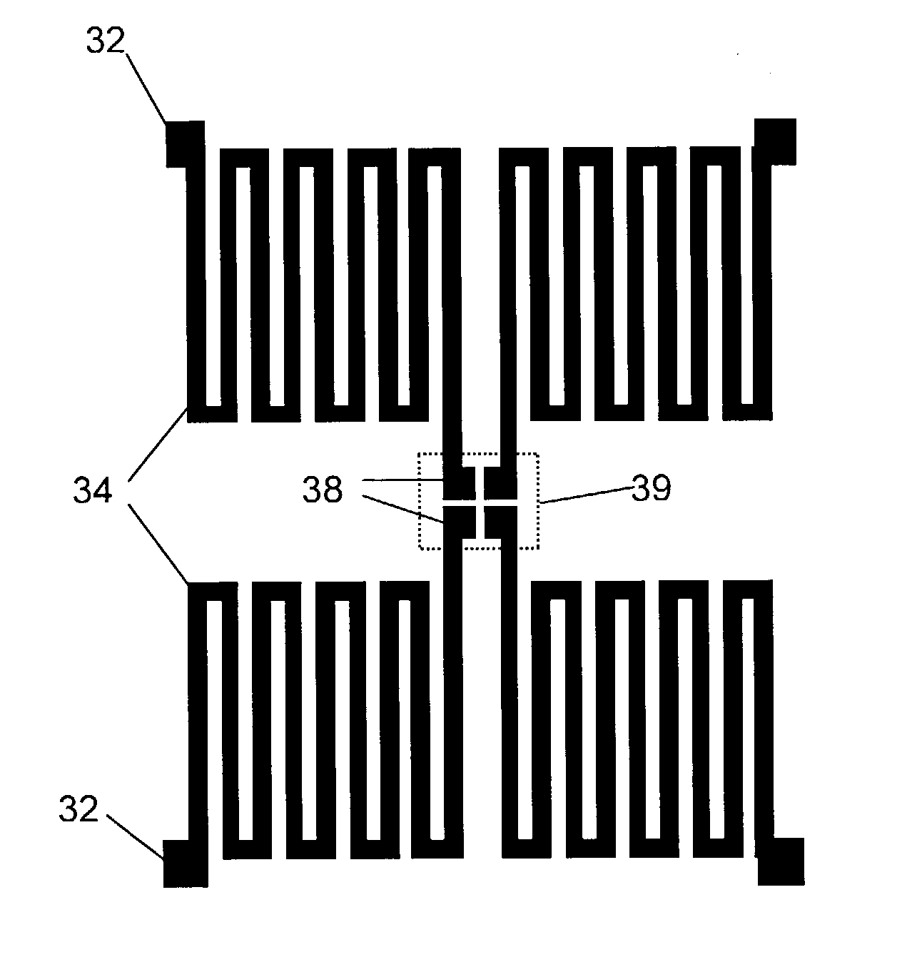
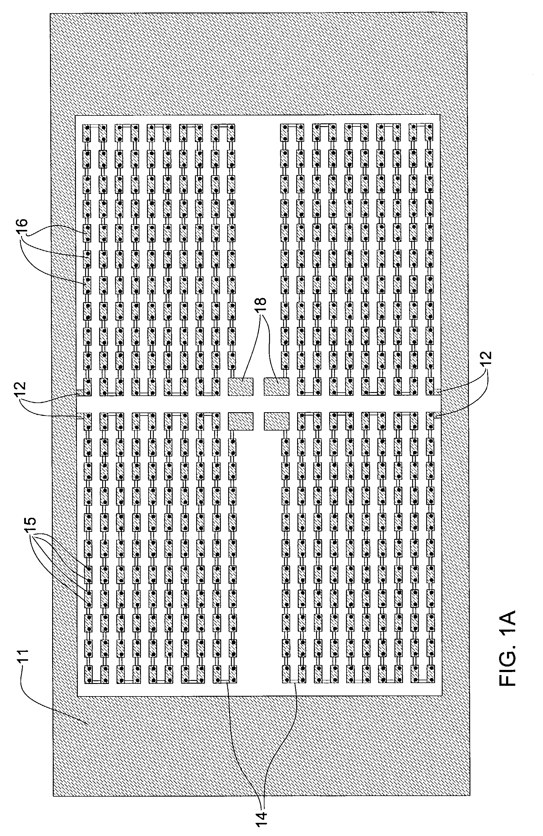
[0019]FIG. 1A shows, by way of example, a pattern of a particular test structure according to the invention, designed to test for discontinuities, i.e. faulty open-circuit conditions, in interlayer connections (vias). The pattern is sized, along one dimension, to fit within a scribe-line; the size along the other dimension may be any. The structure consists of four conductive circuits 14, symmetrically arranged in respective quadrants of the rectangular pattern. Each circuit consists of a large number of conducting segments 16 on each of two layers, only the upper one of which is shown; the segments on the lower layer are schematically represented in the drawing by short lines appearing to connect between the upper segments. The segments are connected in series, alternatingly between the layers, through vias 15, to form a single conductive chain. One end of each chain (i.e. circuit) is connected to a virtual ground 11, at points 12, and the other end is connected to a pad 18 near th...


PUM

PropertyMeasurementUnit
electricallyaaaaaaaaaa
sizeaaaaaaaaaa
electrical stateaaaaaaaaaa

Abstract

A method for electrically testing a semiconductor wafer during integrated-circuit fabrication process, the method including: (i) providing a scanning charged-particle microscope (SCPM), having a defined scanning plane and operative, while in any one mechanical state, to scan a surface in the scanning plane within a two-dimensional scanning window, which has a given maximum size; (ii) providing in association with any layer of the wafer, it being a test layer, one or more test structures, each test structure including normally conductive areas within a normally non-conductive background in one or more layers, which include said test layer, the conductive areas formed as one or more patterns; the patterns in said test layer include one or more clusters of mutually isolated pads; each pad is conductively connected with a corresponding distinct point on the patterns and all the pads in any one cluster are sized and arranged so that at least a significant portion of each pad falls within a common window whose size does not exceed said maximum size of said scanning window; (iii) with said test layer forming the top surface of the wafer, placing the wafer on the SCPM and adjusting the mechanical state of the SCPM so that at least a significant portion of each pad in any one of said clusters is within said scanning window; (iv) causing the SCPM, while in said mechanical state, to scan all of the pads of said one cluster and thereby to provide information about the electrical state of the respective test structure.

Description

FIELD OF THE INVENTION[0001]This invention relates to inspecting and testing semiconductors wafers during circuit fabrication and, in particular, to test structures for electrical testing with an electron beam in voltage-contrast mode.BACKGROUND OF THE INVENTION[0002]Routine inspection of the surface of semiconductor wafers during the fabrication of integrated circuits thereon is commonly carried out by a combination of optical inspection of the entire surface and high-resolution electron beam inspection of suspected spots. Characterization of apparent defects detected during such inspection operation must be correlated with actual faults in the fabricated circuits. Such a correlation is obtained, with respect to any particular fabrication process, by the inclusion of suitable electrical test structures in one or more layers of the wafer. The test structures undergo the same processing as the other circuits and are inspected by the aforementioned means. In addition, however, they ar...

Claims


Application Information

Patent Timeline
Patent Type & Authority Patents(United States)
IPC IPC(8): H01L21/00G01R31/26G01R33/02H01L21/66H01L23/58G01N23/225H01L23/544
CPCG01N23/2258H01L22/34
Inventor BEN-PORATH, ARIELHENDRICKS, DOUGLAS RAY
Owner APPL MATERIALS ISRAEL LTD
Why Eureka
Try Eureka